In order to prevent the power supply user from accidentally connecting the input power line incorrectly and causing the power supply to burn out, an anti-reverse connection circuit is generally required at the power supply input end. At the same time, in order to ensure that the input voltage is within a safe range, the input voltage also needs to be protected against overvoltage cutoff.
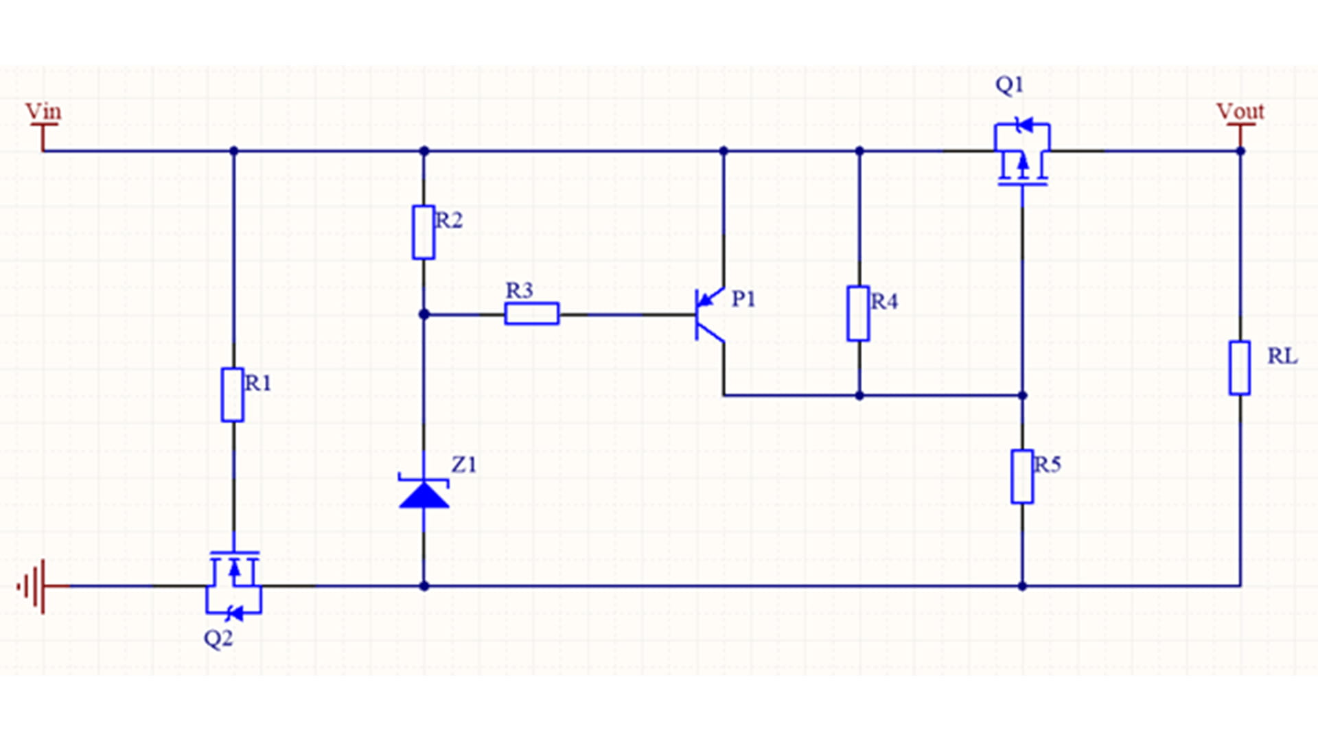
The circuit shown in Figure 1 realizes the integrated function of anti-reverse connection and overvoltage protection.
Its overvoltage protection function is analyzed as follows: When Vin is in the normal input voltage range, the voltage regulator Z1 does not reversely break down, the current of R2 and R3 is basically 0, the Vbe of the transistor P1 is 0, that is, the PNP transistor is not turned on, and the Vgs of the PMOS tube Q1 is determined by the voltage divider of resistors R4 and R5. Vgs is greater than the conduction threshold, and the PMOS tube is turned on, that is, the power supply works normally; when the Vin input is greater than the normal input voltage, at this time Vin>Vbr, the voltage regulator is broken down, the PNP transistor Q1 is turned on, VCE≈0, that is, the Vgs of the PMOS tube is ≈0, and the PMOS tube is turned off, that is, overvoltage protection is achieved.
Its reverse connection protection function is analyzed as follows: the input reverse connection protection is realized by NMOS tube Q2. When the positive pole of the power supply is input from Vin, the gate voltage Vgs of NMOS tube Q2 is high. At this time, Q2 is turned on, Q1, load RL and Q2 form a loop, and the circuit works normally; when the positive pole of the power supply is reversed from the negative terminal below, Q2 is cut off, the entire loop is disconnected and the circuit does not work, thereby playing a role in reverse connection protection.


Xml Privacy Policy Blog Sitemap
copyright @ Micro-Magic Inc All Rights Reserved.
 Network Supported
