

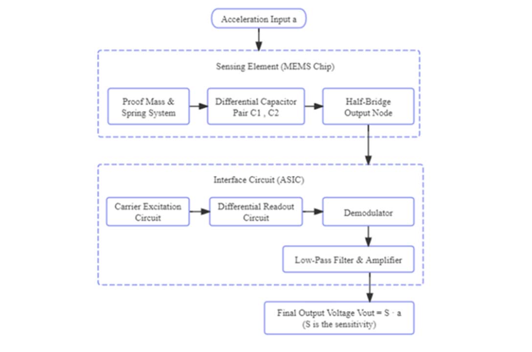
In differential capacitive accelerometers, the core design is a "sandwich" structure: a movable sensitive mass block in the middle (as a common electrode), and fixed electrodes on the upper and lower sides. When there is no acceleration, the mass block is located in the center, and the upper and lower capacitors are equal: When the acceleration α acts along the sensitive axis direction, the inertial force causes the mass block to produce displacement . At this time, the upper and lower capacitors become: The design scheme usually uses a differential half bridge circuit to extract signals. The relationship between output voltage and capacitance difference is: Substitute the above capacitance expression: Therefore, a concise linear relationship is obtained: Combined with the mechanical equilibrium equation (where k is the stiffness of the elastic beam), the final result is: The brilliance of this design scheme lies in the fact that the output is strictly proportional to the acceleration α, and the denominators and can be precisely controlled through photolithography accuracy, allowing for precise sensitivity design. Meanwhile, the differential structure eliminates common mode interference (such as temperature drift and power supply fluctuations), making it a very mature solution in engineering.
Read More
Flux gate sensors and Hall effect magnetic sensors are both devices used to measure magnetic fields, but they have significant differences in principle, performance, and application scenarios. Flux gate sensors are based on the nonlinear magnetization characteristics of magnetic core materials. By exciting the magnetic core with high-frequency alternating current, the saturation characteristics of the magnetic core will change when an external magnetic field exists, resulting in the second harmonic component of the induced voltage (related to the strength of the external magnetic field). Flux gate sensors require complex coil structures and signal processing circuits (such as oscillators and demodulation circuits). Hall effect sensors are based on the Hall effect. When current passes through a conductor or semiconductor, a magnetic field perpendicular to the direction of the current will deflect the charge carriers, generating a transverse voltage (Hall voltage). The Hall voltage is directly proportional to the magnetic field strength and current magnitude. Hall effect sensors have a simple structure, typically consisting of semiconductor materials such as gallium arsenide, silicon, etc., and integrated with signal conditioning circuits. The magnetic flux gate sensor has high sensitivity, it can detect extremely weak magnetic fields (as low as nanotesla level, nT), suitable for measuring the Earth's magnetic field (about 30-60 μT). Hall effect sensors have low sensitivity, they are typically used for magnetic field measurements above the millitesla (mT) level, and some high-sensitivity models can reach micro tesla (μT). The accuracy is greatly affected by temperature, and a temperature compensation circuit is needed to improve stability. Flux gate sensors require high-frequency excitation signals and complex circuits, with high power consumption (usually in the milliwatt range). Not suitable for battery powered portable devices. Hall effect sensors have low power consumption (micro watt level), especially digital output types (such as switch mode Hall sensors). Suitable for low-power applications such as mobile phones and smart devices. Therefore, it is necessary to select flux gate sensors for detecting weak magnetic fields (such as geomagnetic navigation, scientific instruments). Low cost, low-power, high-frequency response (such as motor control, consumer electronics) are required to choose Hall effect sensors.
Read More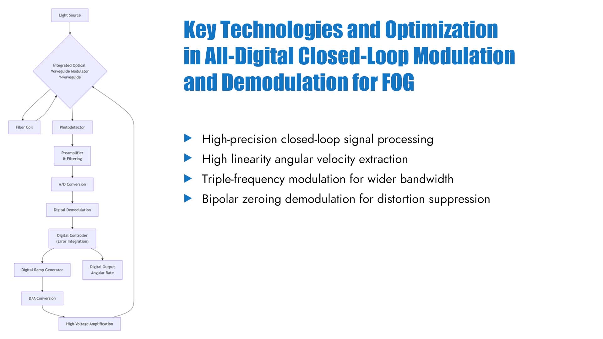
The fully digital closed-loop modulation and demodulation scheme is currently the mainstream technology for high-precision interferometric fiber optic gyroscopes (IFOGs). It modulates and demodulates optical signals under closed-loop conditions through digital circuits, thereby extracting rotational angular velocity with high linearity. A typical fully digital closed-loop signal processing system diagram is shown in the figure below, with key technologies and optimizations including system bandwidth improvement, modulation distortion suppression, and hardware platform implementation. Improvement of System Bandwidth By adopting a triple frequency modulation/demodulation scheme, the sampling period is shortened to one-third of the fundamental frequency scheme, significantly increasing the system bandwidth and better compensating for high-frequency noise signals, improving dynamic performance without affecting static accuracy. Suppression of Modulation Distortion This method adopts a bipolar zeroing pulse square wave demodulation method, which can effectively eliminate or suppress the influence of modulation distortion. Compared to conventional demodulation methods, this technique can reduce the relative error of measuring angular velocity by an order of magnitude (from 1% to 0.1%), which is of great significance for improving the measurement accuracy and stability of closed-loop gyroscopes. Implementation of Hardware Platform All-digital closed-loop schemes typically rely on high-performance digital signal processing platforms. Due to its strong parallel processing capability, high integration, and good flexibility, FPGA has gradually become the mainstream choice. FPGAs can perform all digital demodulation, timing logic control, digital filtering, and even some preprocessing functions. The all-digital closed-loop modulation and demodulation scheme achieves linear extraction of FOG signals through the synergistic operation of phase modulation biasing, digital correlation demodulation, and stepped-wave phase feedback. This scheme is not only key to achieving high precision and a large dynamic range in FOG, but also its adaptability in high-dynamic environments and its level of integration are constantly being improved.
Read More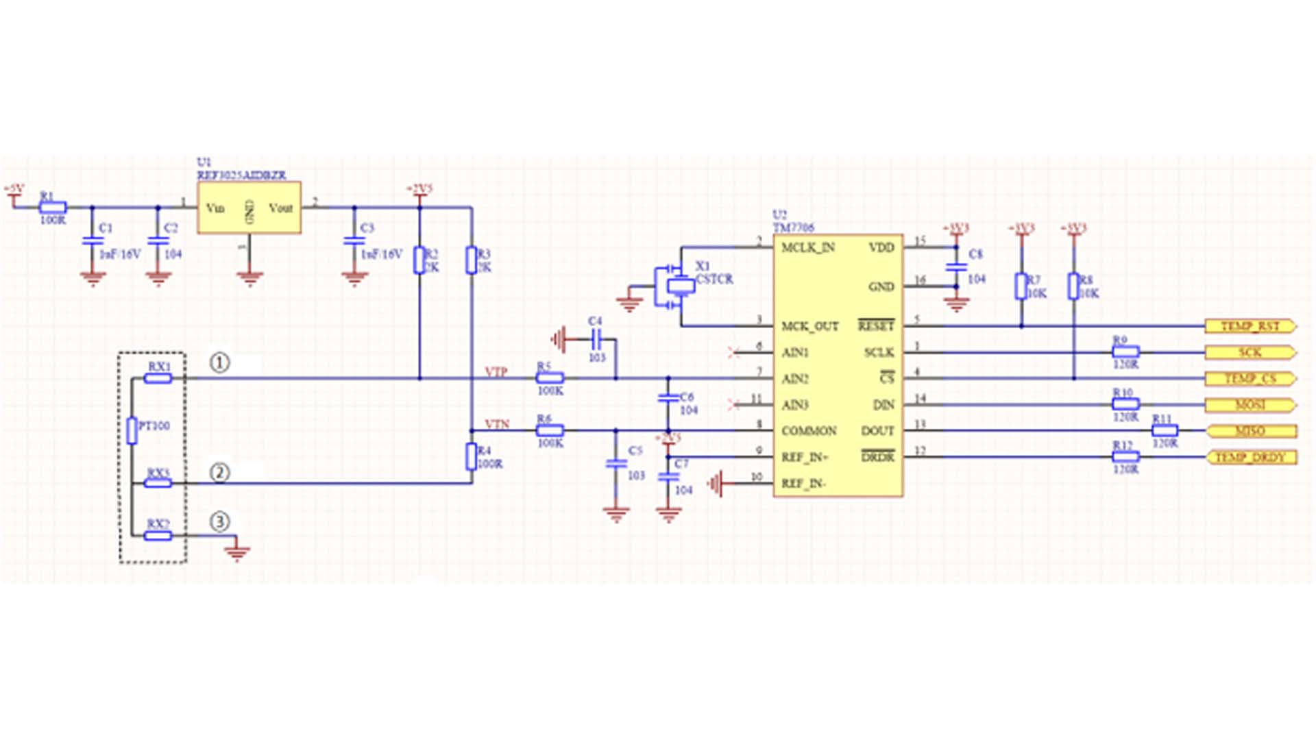
The PT100 resistance thermometer is constructed from pure platinum metal—hence its designation as a platinum resistance thermometer—and stands as the most widely utilized temperature sensor within the medium-to-low temperature range. Its primary characteristics include high measurement accuracy, excellent stability, high reliability, and a long service life. In contrast, thermocouples demonstrate superior performance in high-temperature environments, capable of measuring temperatures reaching as high as 2315°C. The temperature coefficient of platinum resistance is 3.9×10⁻³/°C; at 0°C, its resistance value is 100Ω, and its rate of resistance change is 0.3851Ω/°C. The circuitry typically employed to measure a resistance thermometer is an unbalanced bridge configuration. When the resistance thermometer serves as one of the bridge arms, its connecting lead wires effectively become an integral part of that bridge arm's resistance; since this additional resistance is unknown and fluctuates with ambient temperature, it introduces measurement errors. To eliminate the measurement errors caused by the resistance of these connecting lead wires, a three-wire connection method is commonly adopted. Figure 1 illustrates a three-wire bridge-based sampling and measurement circuit driven by a constant voltage source. The three lead wires extending from the PT100 possess identical cross-sectional areas and lengths, ensuring that their respective lead resistances are equal—specifically, RX1 = RX2 = RX3. One of these wires (RX2) is connected to the bridge's common reference terminal—specifically, the ground terminal—while the remaining two wires (RX1 and RX3) are connected to the bridge arm containing the platinum resistance and the adjacent reference resistance arm, respectively. Through this specific connection scheme, the bridge circuit is able to maintain a balanced state, thereby effectively eliminating the measurement errors attributable to the resistance of the lead wires. In Figure 1 above, resistors R2, R3, and R4, together with the external PT100, form a Wheatstone bridge. The ADC needs only to sample the voltage output of the bridge to calculate the corresponding resistance value of the PT100, thereby deducing the temperature. Under the assumption that lead resistance RX1 equals RX3, the measurement errors introduced by the lead resistances can be effectively cancelled out. The approximate formulas for VT+ and VT- are as follows: VTP = VPT100 + VRX1 + VRX2 VTN = VR4 + VRX3 + VRX2 The voltage difference between points VTP and VTN is: VTP - VTN ≈ VPT100 - VR4 As can be seen, this voltage difference value is independent of the lead resistances; the final voltage difference value can be derived using the following equation: The resistance value of the PT100 can be obtained from the differential pressure value in the above equation.
Read More
With the continuous development of industrial automation technology, accelerometers, as key components, play a crucial role in various automated equipment. To ensure the accuracy and reliability of measurement results, it's essential to select the most suitable accelerometer for a specific application. The following points are key considerations during selection: I. Understanding the Basic Principles of Accelerometers An accelerometer is a sensor that measures the acceleration of an object. Its working principle primarily involves detecting changes in the mass displacement or strain of an object under acceleration. In industrial automation, accelerometers can be used to monitor physical quantities such as vibration, tilt, and impact, thereby achieving real-time monitoring of equipment status. II. Determining the Measurement Range of the Accelerometer When selecting an accelerometer, the first step is to determine its measurement range. The measurement range refers to the maximum acceleration value that the sensor can measure. Based on the requirements of the actual application scenario, select an appropriate measurement range to avoid sensor damage due to an excessively small range or measurement inaccuracy due to an excessively large range. III. Focusing on the Accuracy and Resolution of the Accelerometer Accuracy and resolution are important indicators for evaluating the performance of an accelerometer. Accuracy refers to the deviation between the sensor's output value and the actual value, while resolution refers to the minimum change in the sensor's output signal. In the field of industrial automation, high-precision and high-resolution accelerometers are better suited to meet the high-precision monitoring requirements of equipment status. IV. Consider the Response Frequency of the Accelerometer The response frequency refers to the rate at which the output signal of an accelerometer changes when subjected to a change in acceleration. Select an accelerometer with a suitable response frequency based on different application scenarios. Sensors with high response frequencies can capture acceleration changes more quickly and are suitable for applications with high real-time requirements. V. Choose the Appropriate Installation Method When selecting a sensor, choose an appropriate installation method based on the actual application scenario and equipment structure to ensure stable and reliable sensor operation. VI. Choose the Appropriate Signal Output Method Choose between digital and analog output interfaces based on the characteristics of the application. Digital output interfaces typically include RS232, RS485/RS422, CAN, and TTL level outputs, while analog outputs typically include voltage and current outputs. VII. Consider Environmental Adaptability The environment in industrial automation is complex, and accelerometers need to have strong environmental adaptability. When selecting a sensor, it is important to consider whether it has waterproof, dustproof, and corrosion-resistant features, as well as its operating temperature range, to ensure that the sensor can still function normally in harsh environments.
Read More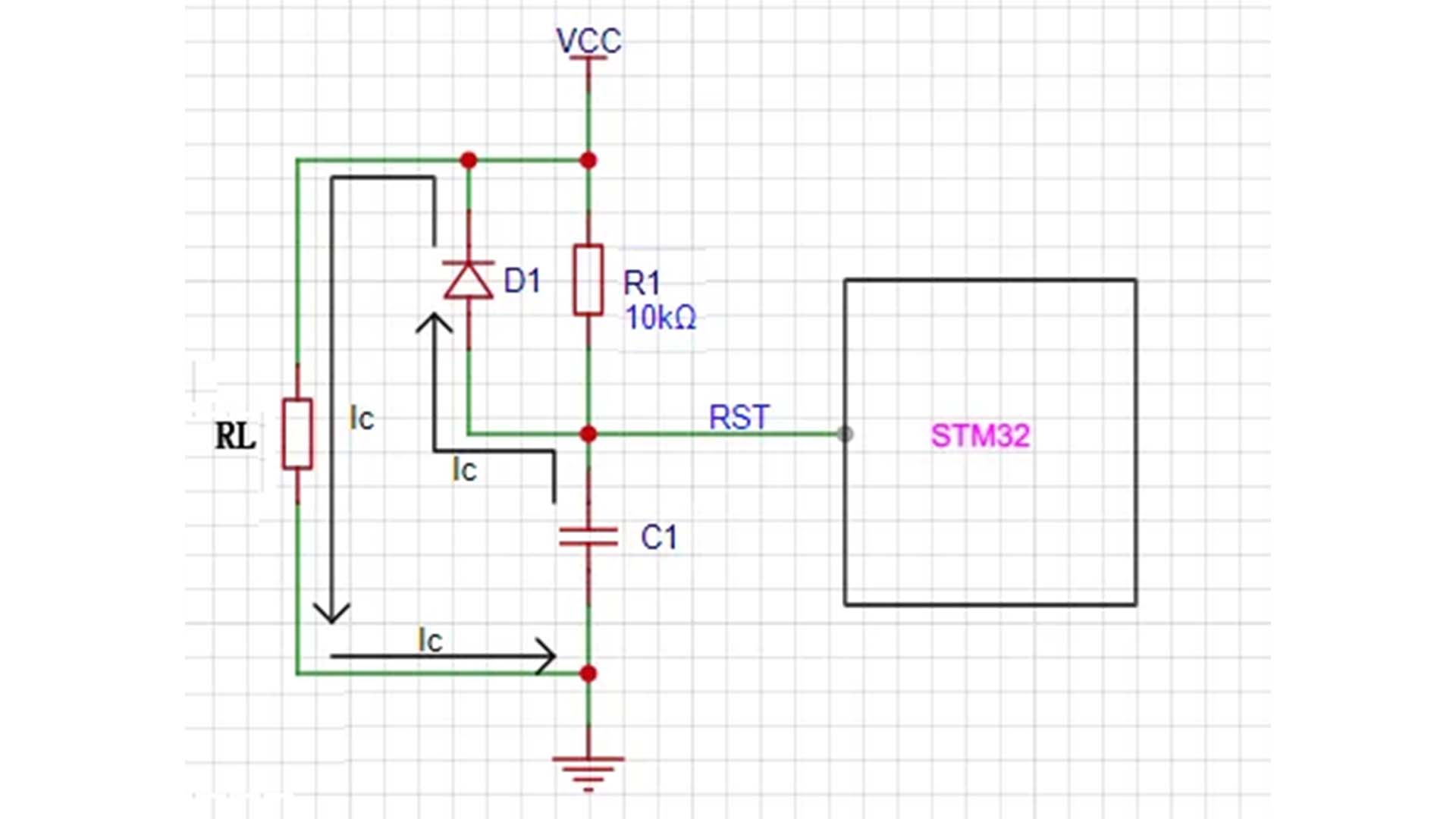
In the STM32 reset circuit shown in Figure 1, a switching diode is usually connected in parallel with the resistor terminal of the RC reset circuit. The main function of this diode is to accelerate the release of capacitor charge. Figure 1 STM32 reset circuit Figure 2 Discharge path of STM32 reset circuit In an RC reset circuit, a discharge diode is indispensable, its main function being rapid discharge. When the power is off or there is a momentary power outage due to interference, the charge stored in the capacitor needs to be released through some path to ensure proper reset upon the next power-on. Without a diode, when the power-off interference pulse is narrow, the capacitor discharges through resistor R1, which has a large resistance, resulting in a slow discharge speed. The RC circuit cannot fully discharge at the moment of power failure, and the system cannot automatically reset upon power restoration. The momentary power outage interference can cause the program to stop running normally, leading to program erratic behavior or entering an infinite loop. The addition of a diode provides a rapid discharge path for the capacitor. Due to the diode's very low on-resistance, as shown in the STM32 reset circuit discharge path in Figure 2, the charge in capacitor C1 discharges rapidly through diode D1, ensuring the stability and reliability of the reset circuit. When the power is off, the capacitor discharges rapidly to ground through the diode. When the power is restored, the capacitor has already discharged completely and can immediately begin the charging process, triggering the reset operation. This rapid discharge process ensures that the reset circuit can quickly return to its initial state after a power outage or abnormal power supply.
Read More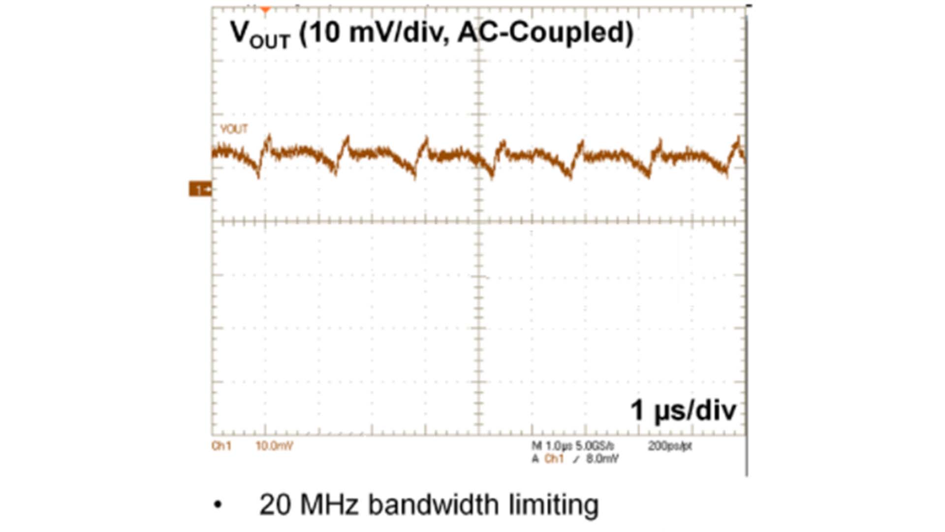
Power supply ripple refers to the periodic AC component appearing at the output of a DC power supply. Its amplitude is usually represented as peak-to-peak or peak-to-valley, as shown in Figure 1. Power supply ripple is mainly caused by waveform imperfections during power conversion, such as voltage changes caused by the switching transistors turning on and off during the operation of a switching power supply. Power supply ripple can affect the normal operation of equipment, especially for precision electronic equipment and analog circuits that require stable power supplies. Figure 1. Power supply ripple and noise Suppressing and reducing power supply ripple to a reasonable range is one of the main goals in power supply circuit design. Therefore, mastering the correct power supply ripple testing methods is crucial for subsequent power supply debugging and ripple design optimization. An oscilloscope is typically used to measure power supply ripple. By setting appropriate trigger conditions and measurement ranges, the waveform and amplitude of the ripple are observed and recorded. Furthermore, other instruments and equipment, such as a ripple coefficient tester, can be used to further analyze and quantify the characteristics of the ripple. To ensure the observation of a true and reliable ripple waveform, the following points should be noted when measuring output voltage ripple using an oscilloscope. The correct method is shown in Figure 2. 1. Select AC coupling mode on the oscilloscope; 2. To ensure signal-to-noise ratio, select X1 for probe attenuation during power supply ripple testing; 3. Set the bandwidth limit to 20MHz to avoid high-frequency noise affecting ripple measurement; 4. Minimize ground loops; a spring grounding ring is recommended as shown on the right side of Figure 2; 5. Place the probe close to both sides of the capacitor; 6. Avoid simultaneously testing waveforms at other points using other oscilloscope channels. Using the correct measurement methods described above will allow you to observe a ripple waveform similar to the one shown below. Figure 3 Ripple waveform
Read More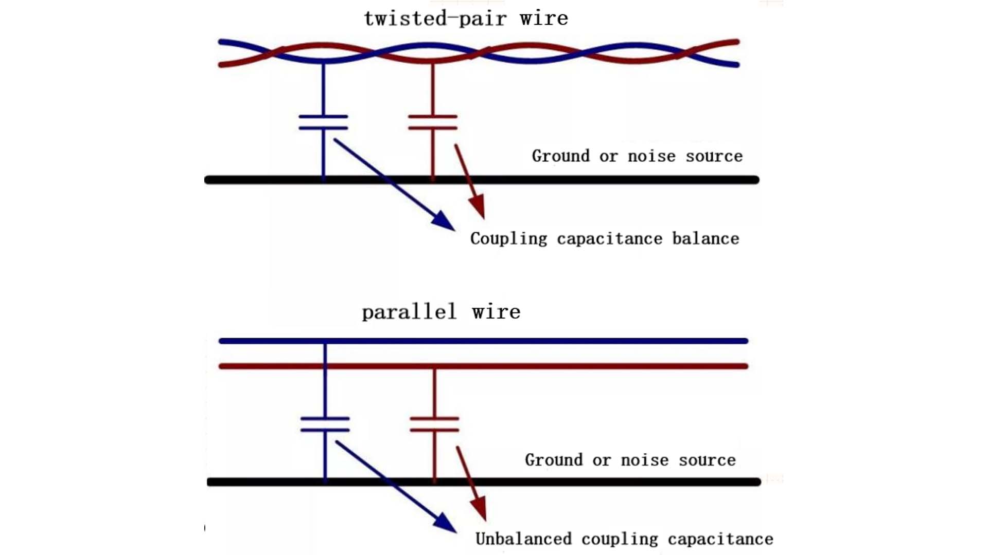
Twisted-pair cable consists of two insulated wires twisted together, making it particularly suitable for differential signal transmission. Compared to parallel wires, it can more effectively suppress interference. The characteristics of twisted-pair cable are reflected in the following two aspects: 1. Elimination of capacitive coupling Compared to parallel wires, the coupling capacitance values of each wire in a twisted-pair cable to the interference source or ground are closer, resulting in a more balanced impedance, as shown in Figure 1. Figure 1 Because the twisted pair wires are tightly wound together, the coupling capacitance between the two wires and the noise source, and the impedance to ground are essentially the same. The interference current flowing from the noise source into the two signal lines is basically identical, and the difference between the two signal lines remains unchanged. The current from the coupling capacitance is converted into common-mode interference. As shown in Figure 2, C1=C2 and Z1=Z2, so the current flowing into C1 and C2 from the interference source is equal, meaning the voltages generated on lines 1 and 2 are equal, and Vn=0. Because the differential signal transmission method has excellent common-mode rejection capability, the effects of capacitive coupling can be eliminated. Figure 2 2. Eliminating Inductive Coupling If parallel lines are used, the two signal lines will form a very narrow loop, which will pick up magnetic field interference from the environment. The structure of a twisted-pair cable involves twisting the two conductors of the transmission line at a fixed interval, causing the direction of the electromotive force induced by the magnetic field to reverse at each adjacent "small loop," thus sequentially canceling it out. From a circuit perspective, the mutual inductance at each adjacent "small loop" is opposite to the noise source, and the overall mutual inductance of the conductors becomes zero. As shown in Figure 3, when parallel lines are subjected to external magnetic field interference, the induced currents in the two conductors cannot cancel each other out, resulting in a large induced voltage that affects signal transmission. The structure of a twisted-pair cable, however, causes the induced currents in the conductors to cancel each other out, preventing the generation of an induced voltage. In differential transmission applications, twisted-pair cables can eliminate capacitive and inductive coupling with external interference sources. Therefore, twisted-pair cables are widely used in differential signal transmission applications such as CAN and RS-485.
Read More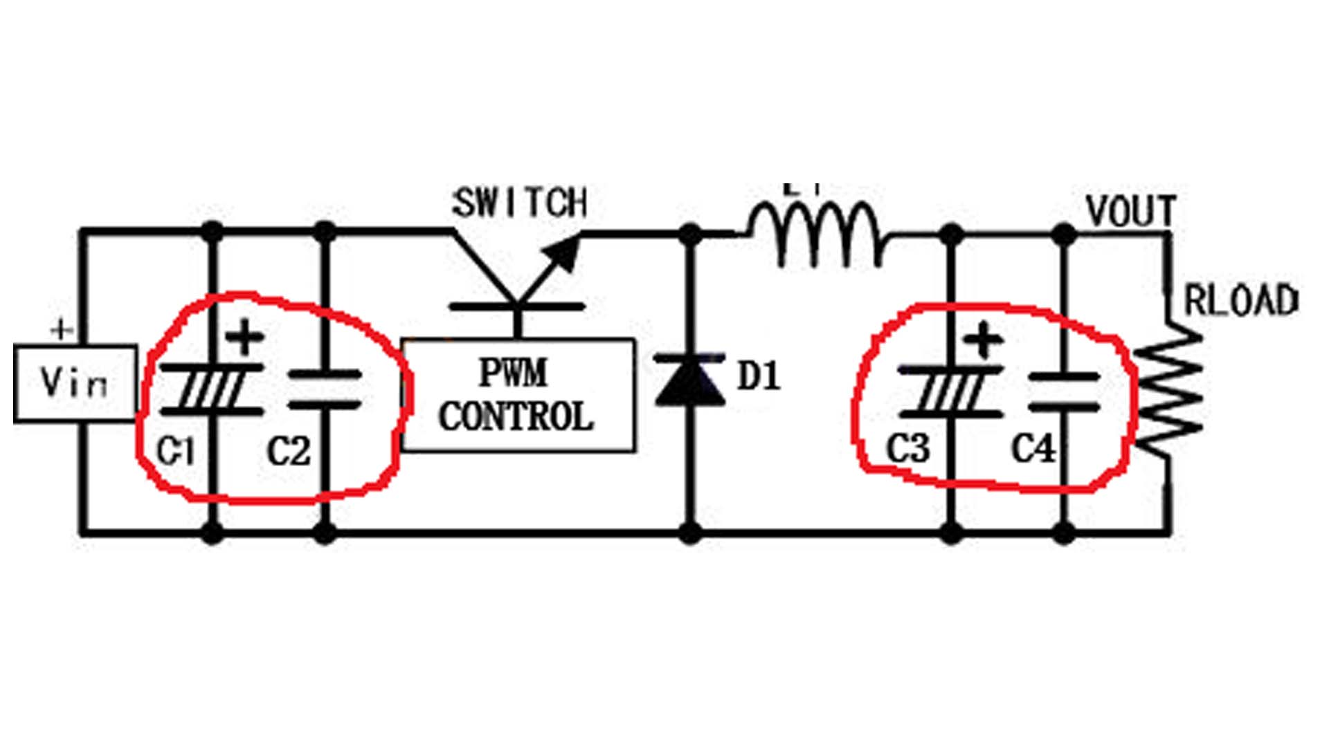
Power supply ripple, or simply ripple, is the periodic fluctuation of voltage or current in a power supply. This fluctuation poses a potential threat to the stable operation of electrical equipment. Excessive power supply ripple can reduce the power system's conversion efficiency, increase heat generation, and in severe cases, lead to system instability or even chip damage. Therefore, when designing a BUCK circuit, measures need to be taken to reduce power supply ripple to ensure system stability. The following are some common methods for reducing BUCK power supply ripple: Increase the inductance and output capacitor for filtering According to the formula for switching power supplies, the magnitude of current fluctuation within the inductor is inversely proportional to the inductance value, and the output ripple is inversely proportional to the output capacitance value. Therefore, increasing the inductance and output capacitance values can reduce ripple. Figure 1 Inductor current Figure 1 above shows the current waveform within the inductor L of a switching power supply. The ripple current ΔI can be calculated using the following formula. Based on volt-second balance and other parameters, it can be seen that increasing the inductor L value or increasing the switching frequency can reduce the current fluctuation within the inductor. Similarly, the relationship between output ripple and output capacitance is: Vripple = Imax/(Co × fsw). It can be seen that increasing the output capacitance value can reduce ripple. Commonly, aluminum electrolytic capacitors are used for the output capacitor to achieve a large capacitance. However, electrolytic capacitors are not very effective at suppressing high-frequency noise, and their ESR is relatively high. Therefore, a ceramic capacitor is connected in parallel next to it to compensate for the shortcomings of aluminum electrolytic capacitors. When a switching power supply is operating, the input voltage Vin remains constant, but the current changes with the switch. When the power supply starts up or the load changes abruptly, an input capacitor is needed as a temporary energy pool to compensate for the instantaneous drop in input voltage. Typically, a capacitor is connected in parallel near the current input terminal (near the switch in a Buck type) to provide current. The input capacitor also suppresses ripple and electromagnetic interference (EMI) from the preceding power supply. After adopting the above solution, the BUCK-type switching power supply is shown in the figure below: Figure 2 BUCK topology The above approach has limited effect on reducing ripple. Due to size limitations, the inductor cannot be made very large; increasing the output capacitor to a certain extent has no significant effect on reducing ripple; and increasing the switching frequency will increase switching losses. Second-stage filtering involves adding another LC filter LC filters are effective at suppressing noise and ripple. By selecting appropriate inductors and capacitors to construct the filter circuit based on the ripple frequency to be removed, ripple can generally be reduced significantly. However, in this case, the sampling point of the feedback comparison voltage needs to be considered. Figure 3 Selecting the sampling point before the LC filter (Pa) will result in a decrease in output voltage. This is because any inductor has a DC resistance, and when current is output, a voltage drop occurs across the inductor, causing the power supply's output voltage to decrease. Furthermore, this voltage drop varies with the output current. Selecting the sampling point after the LC filter (Pb) will produce the desired output voltage. However, this introduces an inductor and a capacitor into the power supply system, potentially affecting loop stability. After the BUCK power output, connect an LDO filter The most commonly used combination is BUCK+LDO, which is the most effective way to reduce ripple and noise. It provides a constant output voltage without requiring changes to the original feedback system, but this also reduces the overall power supply system efficiency and is the most expensive. A key metric for LDOs is PSRR (Power Supply Rejection Ratio), which quantifies the extent to which changes at the power input are transmitted to the output. After passing through an LDO, switching ripple is typically below 10mV. The PCB layout of a switching power supply is also crucial for reducing ripple. Improper component placement, unreasonable grounding, or critical traces being close to the switch-sensitive area can cause increased ripple and high-frequency noise.
Read More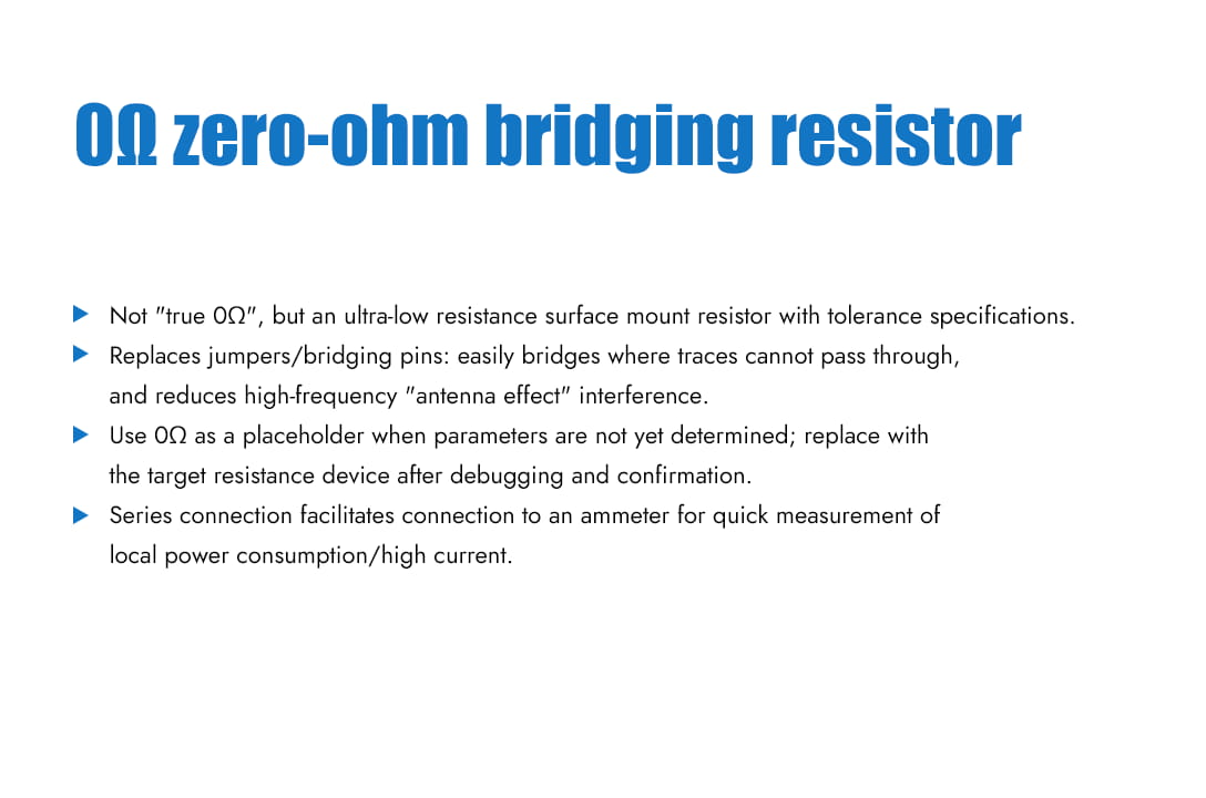
A zero-ohm resistor, also known as a jumper resistor, is a special-purpose resistor. A zero-ohm resistor does not actually have zero resistance; it is a resistor with a very small resistance value. Because it has a resistance value, it has the same tolerance and accuracy specifications as regular surface-mount resistors. In circuit board design, when two points cannot be connected using printed circuits, a jumper is often used on the front side. This is commonly seen in ordinary boards. To ensure the proper functioning of automatic pick-and-place machines and automatic insertion machines, zero-ohm resistors are used instead of jumpers. The functions of a 0-ohm resistor are as follows: 1. It has no function in the circuit; it's only used on the PCB for ease of debugging or design compatibility. 2. It can be used as a jumper to avoid high-frequency interference caused by jumper pins (acting as an antenna). 3. When the matching circuit parameters are uncertain, a 0-ohm resistor can be used as a substitute. During actual debugging, the parameters are determined, and then a component with a specific value is used as a substitute. 4. A 0-ohm resistor is actually a very small resistor. When you want to measure the current consumption of a certain part of the circuit, connect a 0-ohm resistor and an ammeter. This makes it convenient to measure the current consumption and can be used to measure large currents. 5. When routing, if it's impossible to route the circuit, a 0-ohm resistor can be added as a jumper. 6. Under high-frequency signals, it can act as an inductor or capacitor (depending on the characteristics of the external circuit). Inductors are mainly used to solve EMC problems, such as between ground and ground, power supply and IC pads. 7. Single-point grounding, meaning that protective ground, working ground, and DC ground are separated on the equipment, each becoming an independent system. 8. For circuit protection, it can act as a low-cost fuse. 9. Used for current loops when bridging. When the ground plane is split, the shortest return path for signals is broken. The signal loop must then detour, creating a large loop area. This strengthens the influence of electric and magnetic fields, making it easier to interfere with or be interfered with. Connecting a 0-ohm resistor across the split area provides a shorter return path and reduces interference. 10. In mixed-signal circuits such as digital and analog circuits, it is often required that the two grounds be separate and connected at a single point. We can use a 0-ohm resistor to connect these two grounds instead of directly connecting them together. 11. In circuit configuration, jumpers and DIP switches should generally be avoided on products. Sometimes users may tamper with settings, which can easily lead to misunderstandings. To reduce maintenance costs, 0-ohm resistors should be soldered onto the board instead of jumpers.
Read More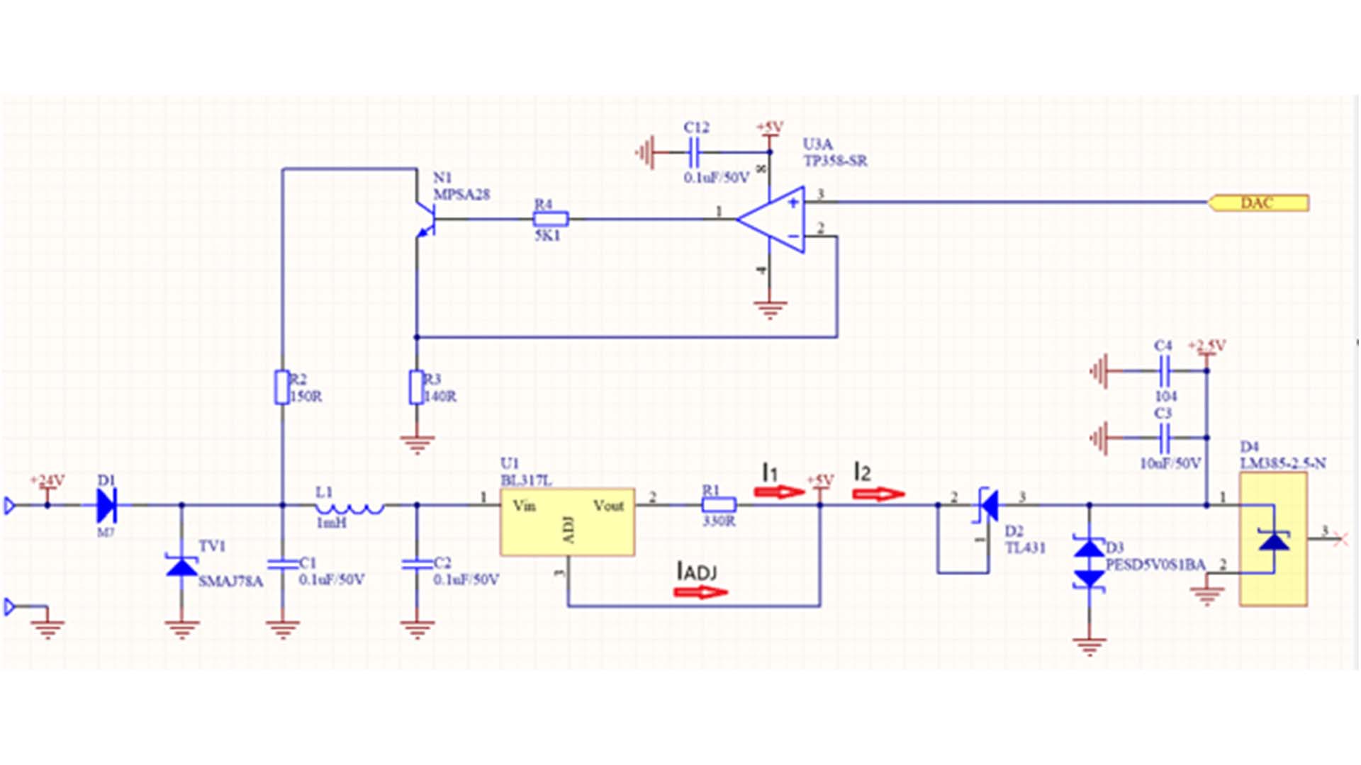
In industrial settings, to save on cabling costs, a 4-20mA two-wire system is commonly used. This system uses two wires to simultaneously power the field sensor/transmitter and transmit the analog signal. We know that the sensor/transmitter circuit requires a certain amount of current to operate; therefore, the circuit structure using this method must be low-power. The 4mA zero-point current ensures that the device can start up and operate normally. The analog signal transmission is achieved by dynamically adjusting a constant current source circuit to ensure that the total current in the loop remains precisely between 4mA and 20mA. Figure 1. Constant current and voltage regulation circuit Figure 2. Internal structure diagram of the LM317 Figure 1 shows a constant current regulator circuit built using the BL317, which is a low-power constant current source circuit that precisely controls the output current to 3.8mA. The circuit ensures that the current flowing into U1 remains constant at 3.8mA, preventing the current from fluctuating with changes in the downstream load. As shown in the internal structure diagram of the LM317 in Figure 2, the voltage between Vout and ADJ remains stable at approximately 1.25V during normal operation, thus the current I1 through resistor R1 also remains constant. The current direction is indicated by arrows, from which the following relationship can be derived: I2 = I1 + IADJ, where IADJ is 50μA and can be neglected. Therefore, I2 is approximately equal to I1, i.e., I2 ≈ I1 = 1.25V/330Ω = 3.8mA. The subsequent stage of the circuit in Figure 1 utilizes the low-power voltage reference diode LM385-2.5 to provide a 2.5V regulated power supply for the low-power system. The LM385-2.5 operates within a current range of 20μA to 20mA and features extremely low dynamic impedance and excellent temperature stability. The circuit also cleverly utilizes the characteristics of the TL431 precision voltage reference source by short-circuiting the reference pin 1 and cathode pin 2 of the TL431 and connecting it in series with the circuit. In this configuration, the voltage drop between the anode and cathode of the TL431 is 2.5V, thus ensuring that the output voltage at the constant current source I2 is 5V. This voltage can provide power for the signal conditioning circuit.
Read More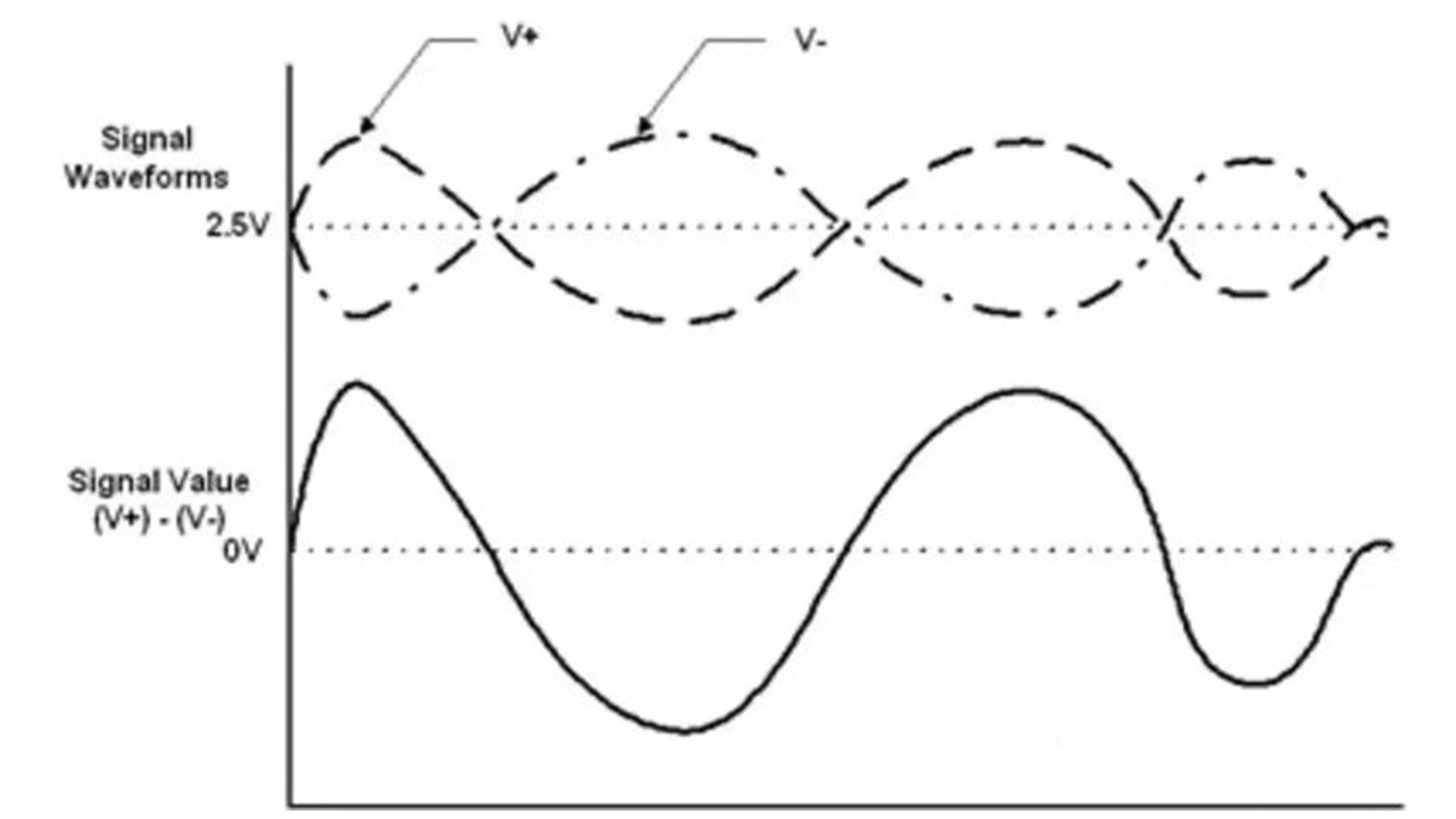
We know that to improve the anti-interference capability of communication systems, RS485, CAN bus, USB, and Ethernet interfaces all use differential signal transmission. Differential transmission is a signal transmission technique that differs from the traditional single-signal-line approach. Differential transmission transmits signals through two lines, with these two signals having equal amplitudes but opposite phases. The signals transmitted on these two lines are called differential signals. A differential signal uses a numerical value to represent the difference between two physical quantities. Differential signals are also called differential-mode signals, as opposed to common-mode signals. Figure 1 shows the transmission waveforms of the V+ and V- differential signals on the signal lines and the data analysis waveforms at the receiving end. Figure 1. Differential signal waveform When we use differential signaling for transmission, although it increases the complexity of any related interface circuits, it offers the following three advantages: 1. Because you are controlling the 'reference' voltage, small signals can be easily identified. In a single-ended signal system using ground as a reference, the accuracy of the measured signal depends on the consistency of the 'ground' within the system. The further the signal source and receiver are from each other, the greater the possibility of differences in their local ground voltage values. The signal value recovered from a differential signal is largely independent of the precise value of the 'ground'; 2. It is highly immune to external electromagnetic interference (EMI). An interference source affects each end of the differential signal pair to almost the same extent. Since the voltage difference determines the signal value, any identical interference appearing on both conductors will be ignored. Besides being less sensitive to interference, differential signals generate less EMI than single-ended signals; 3. In a single-supply system, it can easily and accurately handle 'bipolar' signals. To handle bipolar signals in a single-ended, single-supply system, we must establish a virtual ground at some arbitrary voltage between the ground and the power supply rail (usually the midpoint). Voltages above the virtual ground represent positive signals, and voltages below the virtual ground represent negative signals. Then, the virtual ground must be correctly distributed throughout the system. With differential signaling, such a virtual ground is not needed, allowing us to process and transmit bipolar signals with high fidelity without relying on the stability of the virtual ground.
Read Moreleave a message
Scan to Wechat :