

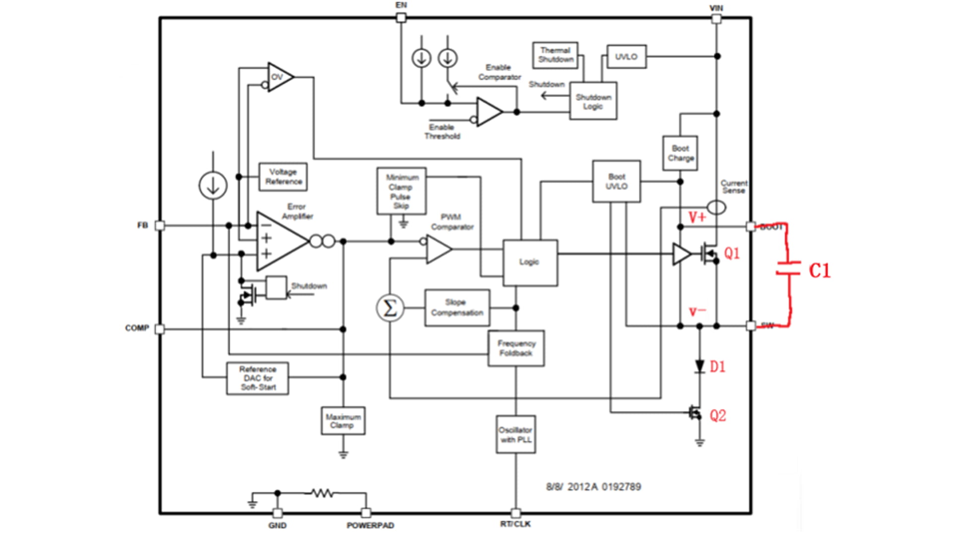
Figure 1 BUC power supply Typically, when designing an asynchronous buck power supply, a bootstrap capacitor is connected between the chip's SW and BOOT pins, such as C1 in Figure 1. The bootstrap capacitor utilizes the characteristic that the voltage across the capacitor cannot change suddenly. When a certain voltage is maintained across the capacitor, when the voltage at the negative terminal of the capacitor is increased, the voltage at the positive terminal remains at the original voltage difference at the negative terminal, thereby increasing the driving voltage. Figure 2 Buck chip internal structure diagram The buck chip shown in Figure 2 consists of two NMOS transistors, which alternately conduct in a complementary manner. The total input voltage VIN is fed through an internal voltage regulator, which outputs a DC low voltage Vb for charging Vboot. This internal voltage regulator is typically a low-dropout (LDO) power supply. During buck chip operation, when the low-side MOSFET Q2 is on, the SW voltage is 0. The LDO output voltage Vb charges the bootstrap capacitor C1, which then flows through the diode D1 and then the low-side MOSFET Q2. The voltage across the capacitor is approximately equal to Vb, and the BOOT pin voltage is now Vb. When the low-side MOSFET Q2 is off and the high-side MOSFET Q1 is on, the voltage at the SW pin rises from 0V to VIN. The S-pole of low-side MOSFET Q2 is directly grounded. As long as the G-pole outputs a high level (>Vth), low-side MOSFET Q2 will turn on. The S-pole voltage of high-side MOSFET Q1 is the input voltage VIN. To maintain the on-state of high-side MOSFET Q1, its gate drive voltage must be greater than VIN + Vgs(th). Since the voltage across the capacitor cannot change suddenly at this point, the BOOT pin is raised to a voltage greater than VIN (VIN + Vb). Capacitor C1 is connected in parallel to the power supply of the high-side MOSFET Q1's driver unit, HS Driver. The bootstrap capacitor C1 discharges to provide power to it, and the supply voltage is the voltage difference across the bootstrap capacitor. Due to the presence of the bootstrap capacitor, the gate-source drive voltage of high-side MOSFET Q1 meets the turn-on condition (Vgs > VIN + Vgs(th)), thus maintaining the on-state of high-side MOSFET Q1. As long as the voltage from the BOOT pin to the SW pin is above the BOOT UVLO threshold, high-side MOSFET Q1 remains on. When the voltage of the bootstrap capacitor drops below the BOOT UVLO threshold due to discharge, the high-side MOSFET Q1 is turned off and the low-side MOSFET Q2 is turned on, periodically charging the bootstrap capacitor, thereby implementing the PWM control mode of the buck power supply.
Read More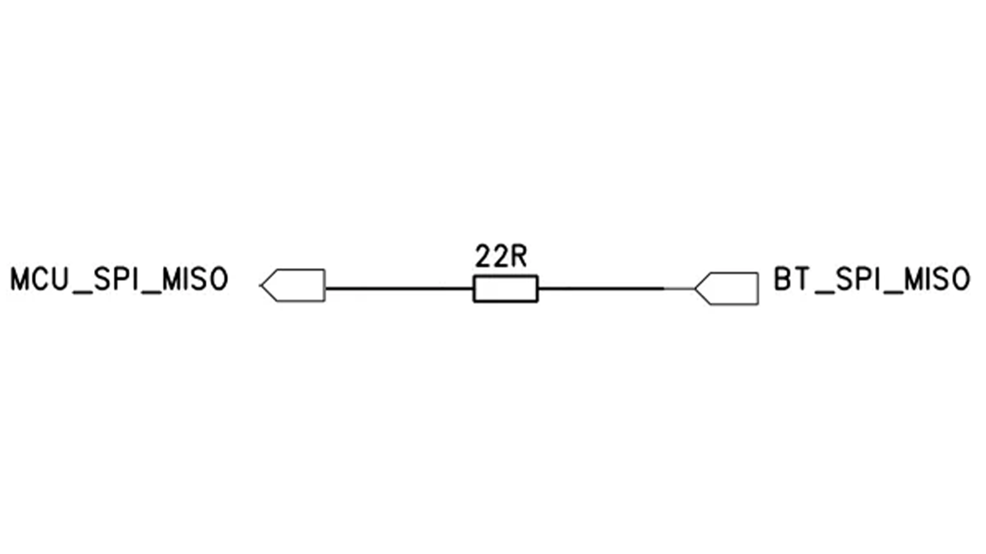
In circuits used for SPI bus communication with peripheral devices, a small resistor with a resistance of tens of ohms is typically connected in series with the signal line, as shown in Figure 1. This design achieves the following functions: 1. Impedance matching. When SPI signal lines are long or the load capacitance is large, the signal may be reflected at the end of the transmission line, causing waveform oscillation (ringing) or overshoot/undershoot. The series resistor acts as an impedance match at the source end (usually close to the master end), absorbing reflected energy and reducing signal integrity issues. This is particularly critical in high-speed SPI (e.g., tens of MHz) or long traces. 2. Reduce electromagnetic interference (EMI). SPI communication often operates at high speeds. The series resistor, along with the capacitance of the line and the load capacitance, forms an RC circuit. This circuit structure helps slow down the rising and falling edges of the signal, thereby preventing overshoot. This has a positive effect on EMI suppression, especially in high-speed circuits. 3. Current limiting and device protection. The resistor limits current flow in the event of an accidental short circuit (e.g., due to wiring errors), preventing damage to the master or slave device I/O ports. 4. Optimize debugging. During debugging, it's common to use an oscilloscope to capture waveforms. Connecting a resistor in series with the SPI signal line makes it easier to observe and debug the signal waveform using an oscilloscope, improving debugging efficiency.
Read More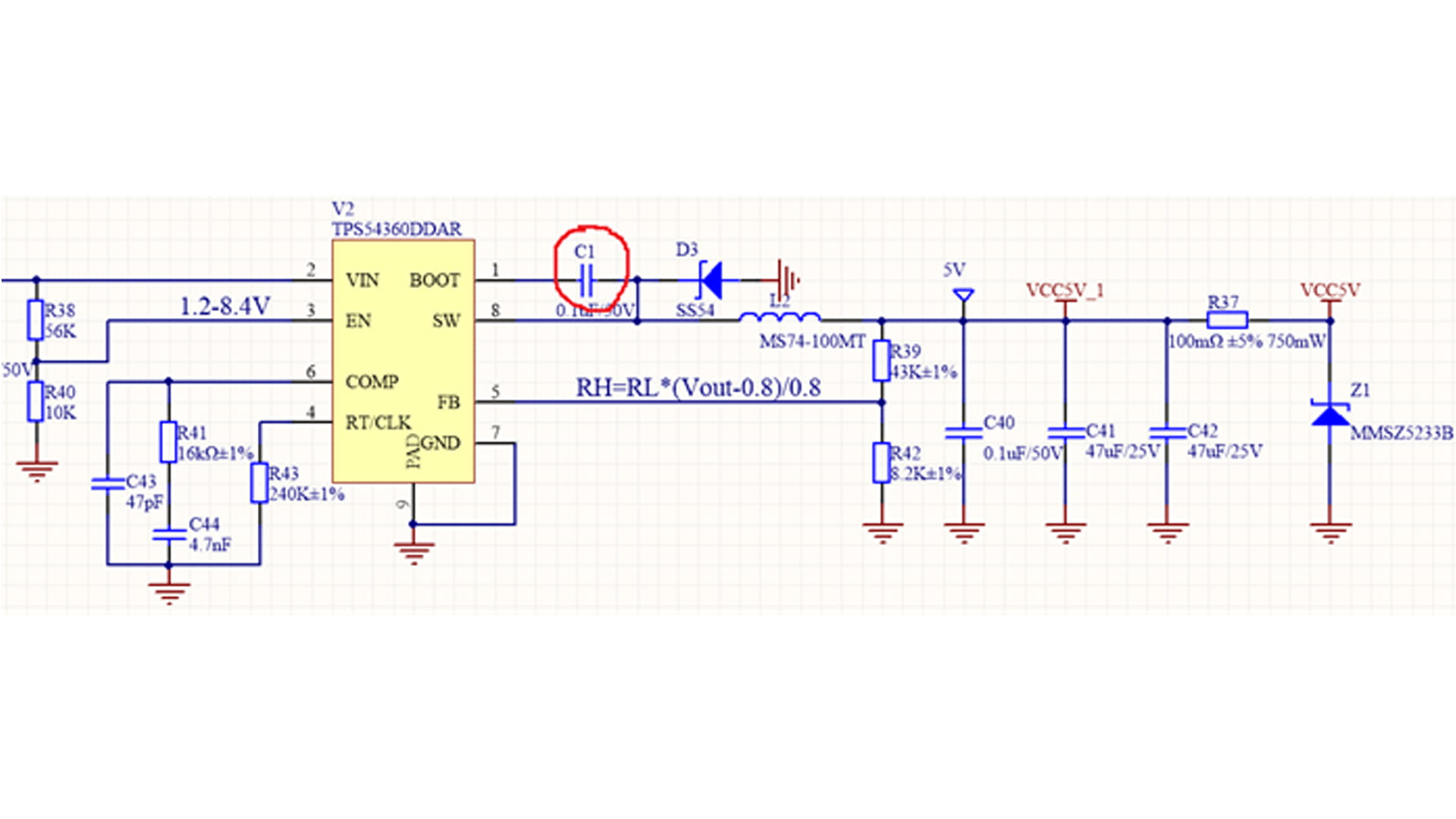
Figure 1 BUC power supply Typically, when designing an asynchronous buck power supply, a bootstrap capacitor is connected between the chip's SW and BOOT pins, such as C1 in Figure 1. The bootstrap capacitor utilizes the characteristic that the voltage across the capacitor cannot change suddenly. When a certain voltage is maintained across the capacitor, when the voltage at the negative terminal of the capacitor is increased, the voltage at the positive terminal remains at the original voltage difference at the negative terminal, thereby increasing the driving voltage. Figure 2 Buck chip internal structure diagram The buck chip shown in Figure 2 consists of two NMOS transistors, which alternately conduct in a complementary manner. The total input voltage VIN is fed through an internal voltage regulator, which outputs a DC low voltage Vb for charging Vboot. This internal voltage regulator is typically a low-dropout (LDO) power supply. During buck chip operation, when the low-side MOSFET Q2 is on, the SW voltage is 0. The LDO output voltage Vb charges the bootstrap capacitor C1, which then flows through the diode D1 and then the low-side MOSFET Q2. The voltage across the capacitor is approximately equal to Vb, and the BOOT pin voltage is now Vb. When the low-side MOSFET Q2 is off and the high-side MOSFET Q1 is on, the voltage at the SW pin rises from 0V to VIN. The S-pole of low-side MOSFET Q2 is directly grounded. As long as the G-pole outputs a high level (>Vth), low-side MOSFET Q2 will turn on. The S-pole voltage of high-side MOSFET Q1 is the input voltage VIN. To maintain the on-state of high-side MOSFET Q1, its gate drive voltage must be greater than VIN + Vgs(th). Since the voltage across the capacitor cannot change suddenly at this point, the BOOT pin is raised to a voltage greater than VIN (VIN + Vb). Capacitor C1 is connected in parallel to the power supply of the high-side MOSFET Q1's driver unit, HS Driver. The bootstrap capacitor C1 discharges to provide power to it, and the supply voltage is the voltage difference across the bootstrap capacitor. Due to the presence of the bootstrap capacitor, the gate-source drive voltage of high-side MOSFET Q1 meets the turn-on condition (Vgs > VIN + Vgs(th)), thus maintaining the on-state of high-side MOSFET Q1. As long as the voltage from the BOOT pin to the SW pin is above the BOOT UVLO threshold, high-side MOSFET Q1 remains on. When the voltage of the bootstrap capacitor drops below the BOOT UVLO threshold due to discharge, the high-side MOSFET Q1 is turned off and the low-side MOSFET Q2 is turned on, periodically charging the bootstrap capacitor, thereby implementing the PWM control mode of the buck power supply.
Read More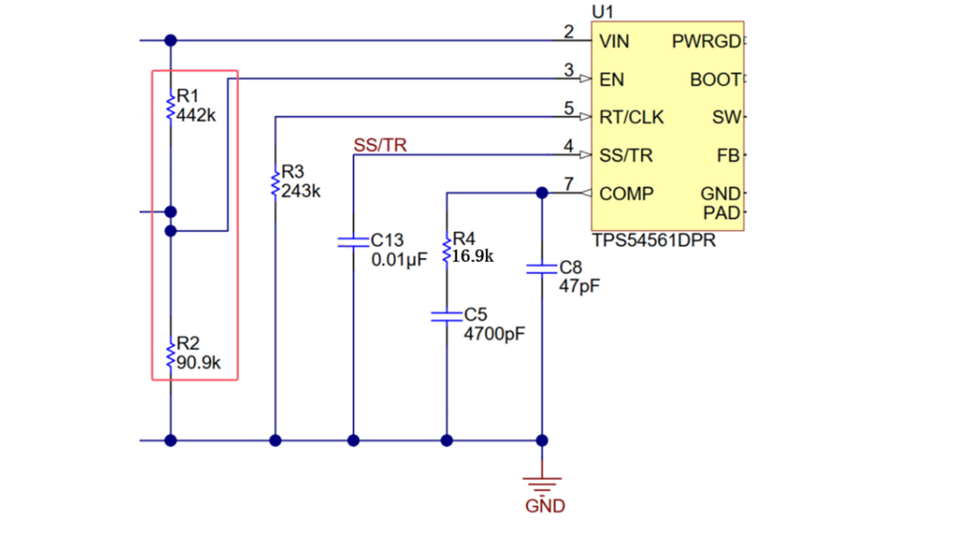
Sensors and instruments all have an operating voltage range, and only within this voltage range can the system operate stably and reliably. We know that the high-voltage threshold can be controlled by an overvoltage protection circuit, but how is the low-voltage threshold defined? Power supplies typically use a buck-type (BUCK) + low-dropout (LDO) solution. The minimum operating voltage is established by the buck-type circuit's UVLO (undervoltage lockout) function, acting as a "safety gate." This ensures that the system operates only when the input voltage is above the UVLO voltage, preventing instability in downstream power supplies and potentially causing system outages due to excessively low input voltages. Undervoltage lockout (UVLO) is a circuit protection mechanism that monitors the system's input voltage. When the input voltage falls below a set threshold, UVLO shuts down the power supply output, preventing system instability, component damage, and even safety hazards caused by insufficient voltage. UVLO Dual Threshold Design Start Threshold (V_START): When the input voltage rises to this value, the circuit begins operating (for example, 6.5V). Shutdown Threshold (V_STOP): When the input voltage drops to this value, the circuit stops operating (for example, 5V). Hysteresis voltage (HYS): This prevents frequent switching caused by voltage fluctuations near the threshold (for example, after starting at 6.5V, the voltage must drop to 5V before shutting down). Take TI's TPS54561 buck power supply chip as an example. Its UVLO function is implemented through the EN pin. Its internal structure includes two key modules: ① Voltage comparator: This detects the EN pin voltage against an internal threshold (typical value V_ENA = 1.2V). ② Hysteresis current source: This provides a hysteresis current of Ihys = 3.4μA to prevent frequent switching caused by voltage fluctuations. According to the datasheet, the TPS54561 EN pin includes a pull-up current source I1 = 1.2μA, a hysteresis current source Ihys = 3.4μA, and V_ENA = 1.2V (EN pin threshold). The UVLO threshold is configured using two voltage-divider resistors, as shown in the following formula: TPS54561 UVLO Configuration Method Use an external resistor divider network to adjust the UVLO start voltage (V_START) and shutdown voltage (V_STOP): Start when the input voltage is ≥ 6.5V (add 1-3V steps to the output voltage target of 5V, here 5V + 1.5V = 6.5V). Stop when the input voltage is ≤ 5V (because the output voltage target is 5V). Calculation Steps: Calculate R1/R_UVLO1: R_UVLO1 = (V_START - V_STOP) / I_HYS = (6.5V - 5V) / 3.4μA ≈ 442kΩ Calculate R2/R_UVLO2: R_UVLO2 = (V_ENA * R_UVLO1) / (V_START - V_ENA + I1 * R_UVLO1) ≈ 90.9kΩ The final result is shown in the figure below: UVLO acts like a watchdog for the power supply system, taking decisive action when voltage is abnormal, adding a safety lock to your power supply solution!
Read More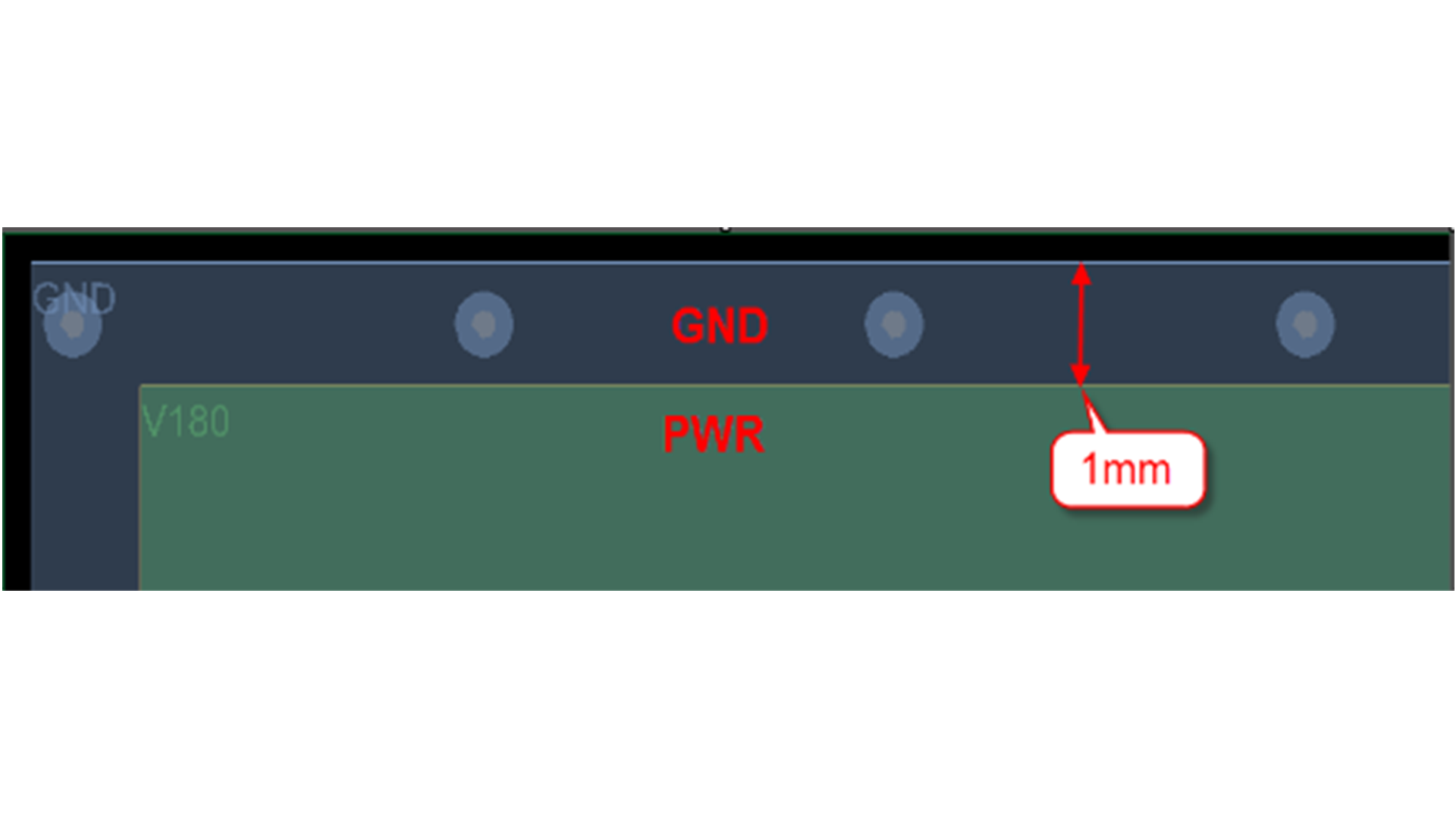
When designing high-speed or high-frequency PCBs, electronics engineers use the 20H principle to meet EMI standards and reduce electromagnetic radiation. This principle requires the power plane to be set back 20H relative to the ground plane, where H represents the distance between the power plane and the ground plane. This also serves to suppress edge radiation. Electromagnetic interference radiates outward at the board's edges. By setting the power plane back, the electric field is conducted only within the confines of the ground plane, effectively improving EMC. A 20H backing can confine 70% of the electric field to the ground edge; a 100H backing can confine 98% of the field. The ground plane should be larger than the power or signal plane to prevent external radiation interference and shield the ground plane from external interference. Generally, setting the power plane back 1mm relative to the ground plane during PCB design is sufficient to meet the 20H principle. To implement the 20H principle, we typically set the power plane back 1mm relative to the ground plane when splitting the plane layers. Shielding ground vias, each 150 mil, are then drilled within the 1mm backing tape, as shown in Figure 1.
Read More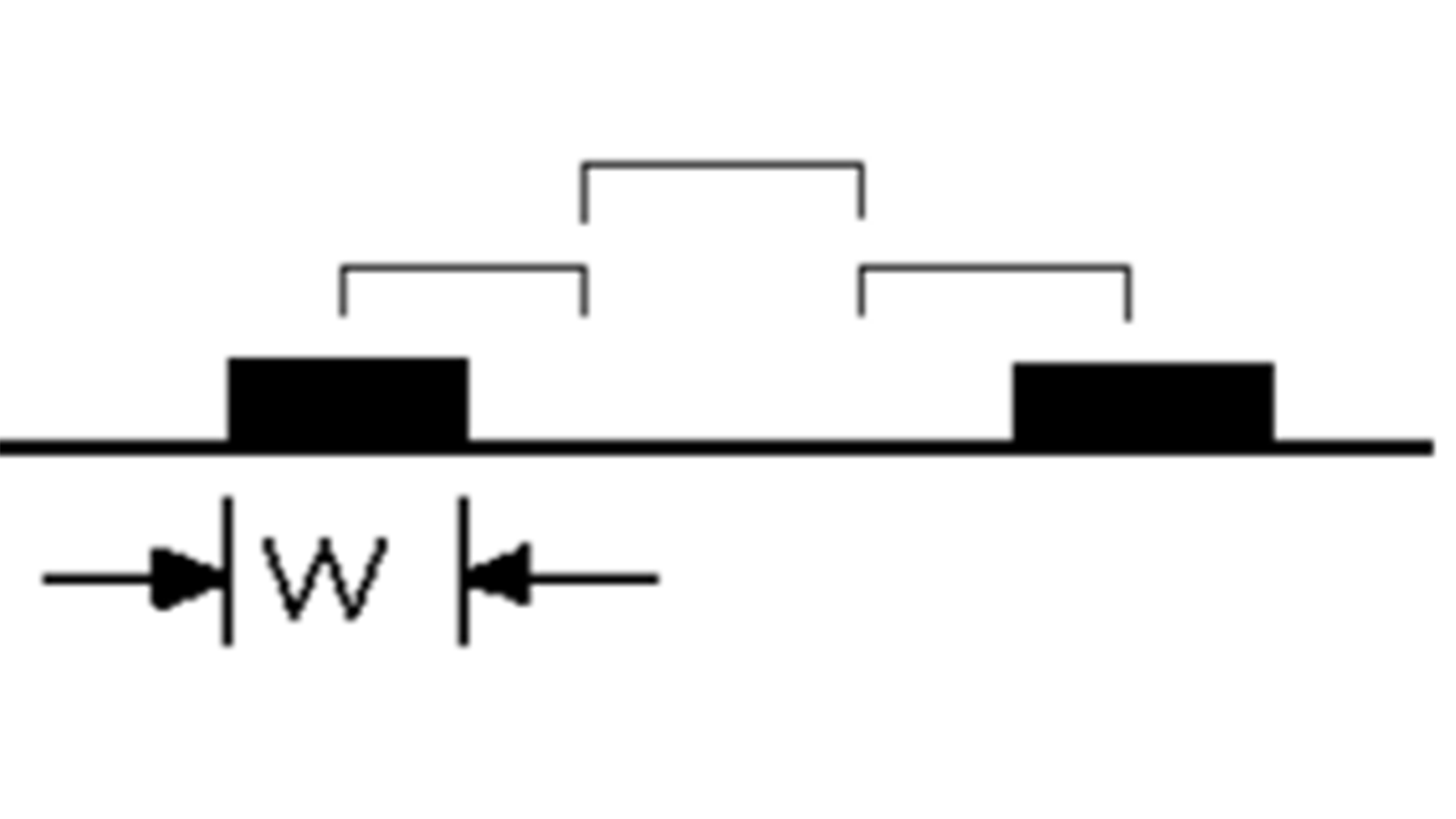
To ensure signal routing quality and prevent crosstalk during PCB design, we maintain a spacing of three times the line width between signal traces. As shown in Figure 1, this spacing refers to the center-to-center spacing of the traces. Because line width is expressed in English as "width," this rule is often referred to as the 3W principle. When the center-to-center spacing of traces is at least three times the line width, 70% of the inter-line electric fields are guaranteed to be free of interference. If 98% of the inter-line electric fields need to be free of interference, the 10W rule can be used. The 3W principle is a PCB layout principle that designers can adhere to without requiring additional design techniques. However, this design approach consumes significant area and can make routing more difficult. The fundamental starting point for the 3W principle is to minimize coupling between traces. This principle can be expressed as follows: the distance between traces (the distance between trace centers) must be three times the width of a single trace. Alternatively, the distance between two traces must be greater than twice the width of a single trace. For example, if a clock line is 6 mil wide, other traces can only be routed 2 x 6 mils away from this trace, or the edge-to-edge spacing must be greater than 12 mils. The 3W principle is easily implemented in PCB design by ensuring that the center-to-center spacing between traces is three times the trace width. For example, if a trace is 6 mil wide, then in Allegro, the line-to-line rule can be set to 12 mils to meet the 3W principle. The spacing in the software is calculated based on the edge-to-edge spacing, as shown in Figure 2.
Read More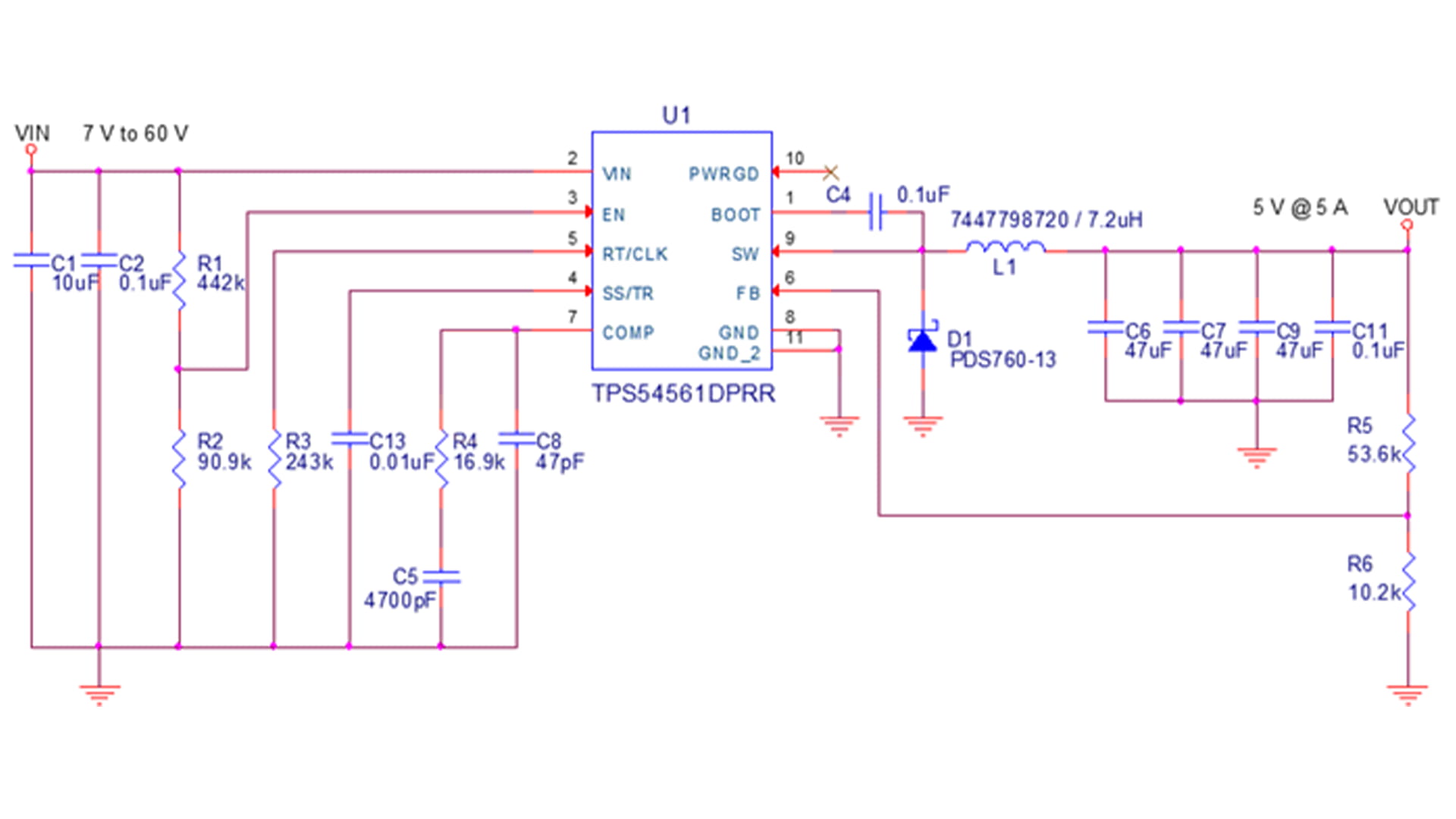
Inrush current is a transient, high current generated when a power supply or device is powered on. In our power supplies and electronic systems, inrush current is undesirable because it can cause device overstress and damage. Buck switching power supply circuits use a soft-start circuit to control the current rise rate during system startup, gradually delivering power to the load and mitigating the impact of inrush current on the system. The soft-start function of a buck power supply is achieved by configuring a soft-start capacitor. This effectively suppresses inrush current, preventing the output capacitor's charging current from exceeding the switching power supply's current limit during startup. This reduces the current surge in the switching circuit itself and downstream loads, and minimizes input voltage drops. Furthermore, a properly configured soft-start time ensures a smooth output voltage rise, avoiding fluctuations . Let's take TI's TPS54561DPRT chip as an example. Its internal functional block diagram is shown in Figure 1. The TPS54561DPRT implements soft-start by connecting an external capacitor to the SS/TR pin. The volt-ampere relationship of a capacitor is expressed as I = C * dV / dt. This shows that the larger the capacitance, the higher the voltage, and the shorter the charging time, the greater the charging current. In other words, for a given capacitance, the magnitude of the capacitor charging current is proportional to the rate of change of the voltage. A typical buck switching power supply device implements configurable soft-start time by connecting an external soft-start capacitor CSS to the soft-start pin SS. The internal pull-up soft-start charging current source ISS charges the soft-start capacitor CSS and then compares it with the reference voltage VREF to determine the end of the soft-start process. According to the capacitor charging formula (I = C*ΔV/ΔT), the time TSS required for the voltage on the soft-start capacitor to charge from zero to VREF is: TSS_SET = CSS * VREF/ISS (Equation 1) For a buck converter circuit, assuming the output voltage setpoint is VOUT, the output capacitor is COUT, and the inrush current charging the output capacitor is IINRUSH, the time required for the voltage on the output capacitor (i.e., the output voltage) to rise from zero to the setpoint VOUT is TSS_OUT. Using the capacitor charging formula, we get: TSS_OUT = COUT * VOUT/IINRUSH (Equation 2) The startup requirement for a switching power supply is that the voltage on the soft-start capacitor must charge from zero to VREF within the soft-start time TSS_SET, and the voltage on the output capacitor must charge from zero to the setpoint VOUT within the same timeframe. Therefore, we get: TSS_SET = TSS_OUT (Equation 3) The final formula for calculating the soft-start capacitor is: (Equation 4) When a switching converter starts up, the current that charges the output capacitor is conventionally referred to as the inrush current, IINRUSH. This current is typically 5% to 10% of the switching converter's maximum load current, IOUT,MAX. If the inrush current, IINRUSH, is 5% of the switching power supply's maximum output current, IOUT,MAX, then IINRUSH = 5% × IOUT. Substituting IINRUSH = 5% × IOUTMAX into Equation 4 yields the following expression for the soft-start capacitor, CSS: (Equation 5) Taking the TPS54561DPRT chip as an example, the actual calculation data is as follows: Requirements: VOUT = 5.0V, COUT = 3 * 47uF = 141uF, IOUT,MAX = 5.0A Parameters: ISS = 1.7uA, VREF = 0.8V, IINRUSH = 5% * 5.0A = 0.25A Calculation results: A standard capacitor close to 10nF is used. This is the reason why C13 = 0.01uF in the figure below. Configuring soft-start capacitors is a key step in suppressing inrush current and ensuring system stability. By properly selecting the capacitor capacity, you can protect components while meeting the startup requirements of different scenarios.
Read More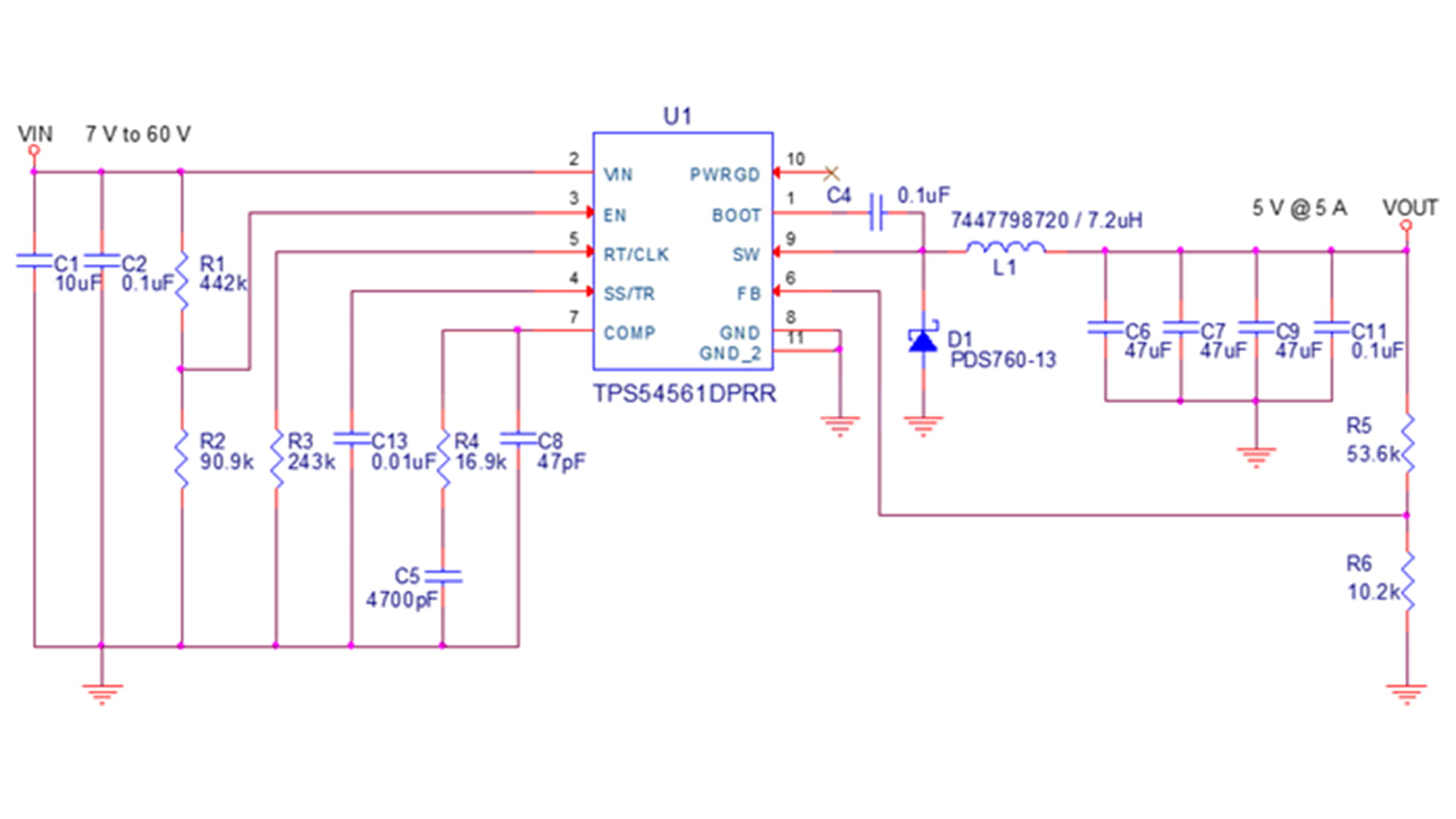
Inrush current is a transient, high current generated when a power supply or device is powered on. In our power supplies and electronic systems, inrush current is undesirable because it can cause device overstress and damage. Buck switching power supply circuits use a soft-start circuit to control the current rise rate during system startup, gradually delivering power to the load and mitigating the impact of inrush current on the system. The soft-start function of a buck power supply is achieved by configuring a soft-start capacitor. This effectively suppresses inrush current, preventing the output capacitor's charging current from exceeding the switching power supply's current limit during startup. This reduces the current surge on the switching circuit itself and downstream loads, and minimizes input voltage drops. Furthermore, a properly configured soft-start time ensures a smooth output voltage rise, avoiding fluctuations. Let's take TI's TPS54561DPRT chip as an example. Its internal functional block diagram is shown in Figure 1. The TPS54561DPRT implements soft-start by connecting an external capacitor to the SS/TR pin. The volt-ampere relationship of a capacitor is expressed as I = C * dV / dt. Therefore, the larger the capacitance, the higher the voltage, and the shorter the charging time, the greater the charging current. In other words, for a given capacitance, the magnitude of the capacitor charging current is proportional to the rate of change of the voltage. A typical buck switching power supply device implements configurable soft-start time by connecting an external soft-start capacitor CSS to the soft-start pin SS. The internal pull-up soft-start charging current source ISS charges the soft-start capacitor CSS and then compares it with the reference voltage VREF to determine the end of the soft-start process. According to the capacitor charging formula I = C * ΔV / ΔT, the time TSS required for the voltage on the soft-start capacitor to charge from zero to VREF is: TSS_SET = CSS * VREF / ISS (Equation 1) For a buck converter circuit, assuming the output voltage setpoint is VOUT, the output capacitor is COUT, and the inrush current charging the output capacitor is IINRUSH, then the time required for the voltage on the output capacitor (i.e., the output voltage) to rise from zero to the setpoint VOUT is TSS_OUT. Using the capacitor charging formula, we get: TSS_OUT = COUT * VOUT / IINRUSH (Equation 2) The startup requirement for a switching power supply is that the voltage on the soft-start capacitor is charged from zero to VREF within the soft-start time TSS_SET, and the voltage on the output capacitor is charged from zero to the setpoint VOUT within the same timeframe. Therefore, we get: TSS_SET = TSS_OUT (Equation 3) The final formula for calculating the soft-start capacitor is: (Equation 4) When a switching converter starts up, the current that charges the output capacitor is conventionally referred to as the inrush current, IINRUSH. This current is typically 5% to 10% of the switching converter's maximum load current, IOUT,MAX. If the inrush current, IINRUSH, is 5% of the switching power supply's maximum output current, IOUT,MAX, then IINRUSH = 5% × IOUT. Substituting IINRUSH = 5% × IOUTMAX into Equation 4 yields the following expression for the soft-start capacitor, CSS: (Equation 5) Taking the TPS54561DPRT chip as an example, the actual calculation data is as follows: Requirements: VOUT = 5.0V, COUT = 3 * 47uF = 141uF, IOUT,MAX = 5.0A Parameters: ISS = 1.7uA, VREF = 0.8V, IINRUSH = 5% * 5.0A = 0.25A Calculation results: A standard capacitor close to 10nF is used. This is the reason why C13 = 0.01uF in the figure below. Configuring soft-start capacitors is a key step in suppressing inrush current and ensuring system stability. By properly selecting the capacitor capacity, you can protect components while meeting the startup requirements of different scenarios.
Read More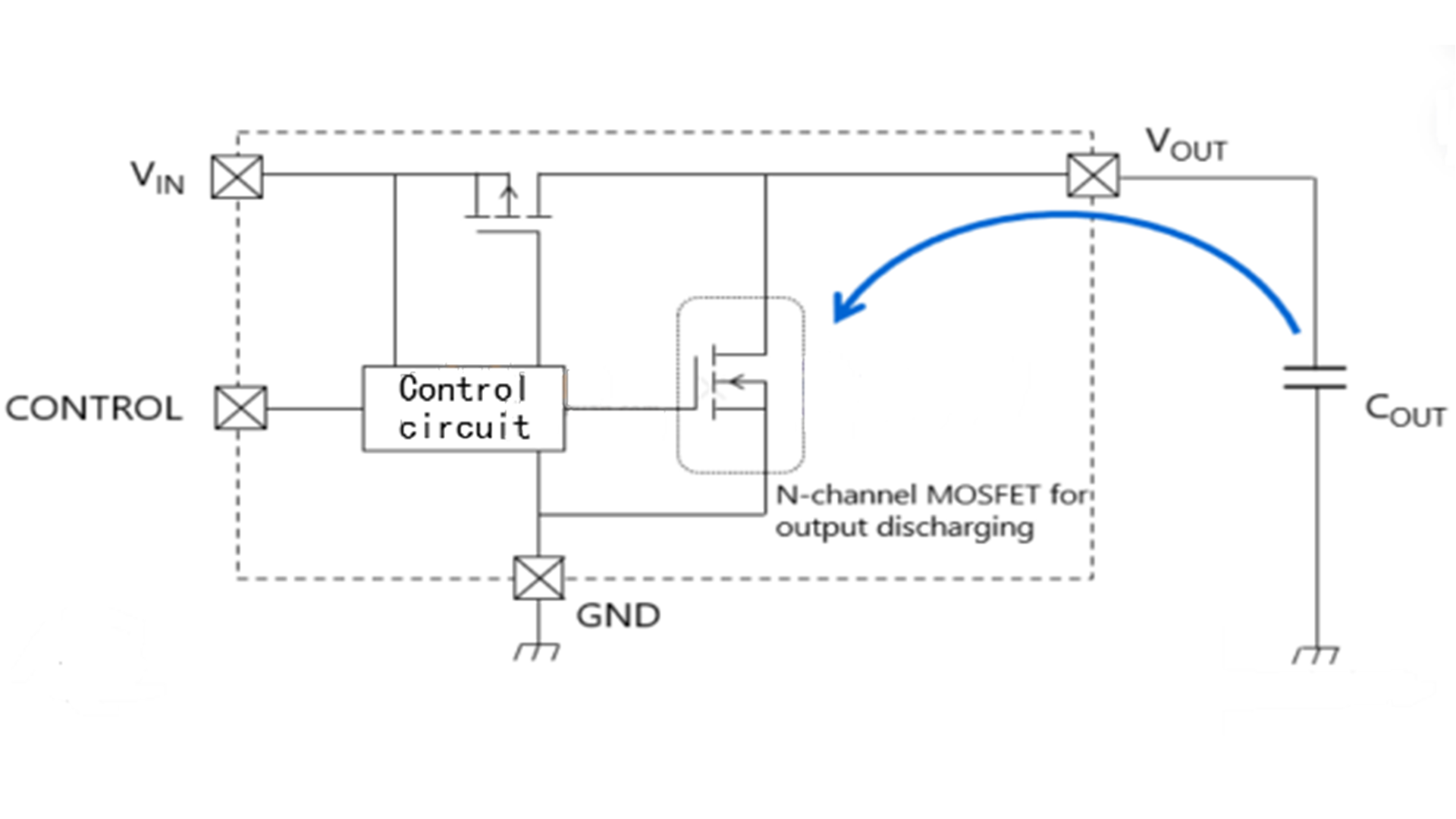
LDOs regulate their output voltage to ensure stable operation under varying load current demands. However, when the load current exceeds the designed range, such as in a short circuit or overload, the excessive current can cause chip overheating or even damage. To address this, overcurrent protection mechanisms have emerged to limit the output current and protect both the LDO and its load. LDOs typically have two overcurrent protection mechanisms: brick-wall current limiting and overcurrent shutdown. 1. Brick-Wall Current Limiting As its name suggests, brick-wall current limiting is a "hard" cutoff mechanism. When the output current exceeds the preset current limit, I_LIMIT, the LDO quickly limits the output current to I_LIMIT. Due to the high load current, the LDO temperature gradually rises. Once the LDO protection temperature is reached, the LDO output is immediately shut down. From the output voltage-output current curve, this resembles a "brick wall" preventing further current increase. For example, the TPS7A16 data sheet indicates that its brick-wall current limit threshold is 105mA (typical). As can be seen from the output voltage-load current curve in the figure above, when the load current exceeds I_LIMIT and triggers the LDO temperature protection, the output voltage drops sharply. This mechanism is typically implemented through an internal current sensing circuit combined with a temperature protection circuit. The LDO's internal structure includes a current mirror to detect current. When the sensed current exceeds the set reference current, the current limit is triggered, the LDO temperature rises, and when it reaches the protection temperature, the power transistor is turned off, cutting off the output. This indicates that brick-wall current limiting is safer during short-term overloads. Its characteristic is that it can tolerate short-term overloads, but if the overload persists, heat accumulation will trigger thermal shutdown. 2. Foldback Current Limit Foldback current limiting is very similar to standard upper-limit limiting. However, its primary purpose is to limit total power dissipation. This means that as VOUT decreases and VIN remains stable, the output current limit is linearly reduced to keep the output transistor within a safe power dissipation limit. Devices such as the TLV717P incorporate and benefit from foldback current limiting because they are primarily housed in ultra-small packages with higher thermal resistance. The output current limit behavior of the TLV717P is shown in Figure 3. As can be seen, since VIN is specified at VOUT + 0.5V, the maximum allowable power dissipation at 25°C is 150mW. After the current limit is exceeded and VOUT begins to decrease (assuming RLOAD is constant), both IOUT and power dissipation decrease. This adds a slight complexity to non-ohmic devices that consume a constant current and can trigger a latched state where the powered device continues to reduce VOUT and the LDO continues to reduce IOUT. 3. Overcurrent shutdown Unlike brick-wall current limiting and foldback current limiting, overcurrent shutdown protection utilizes a fast internal shutdown mechanism. The LDO's internal structure incorporates a current mirror to sense current and a comparator to enable rapid overcurrent output shutdown. When the LDO output current reaches the overcurrent protection current, the LDO directly shuts down. Therefore, current threshold protection is faster than brick-wall current limiting and foldback current limiting. If the LDO output has a large capacitive load, the LDO output will experience a large inrush current, potentially triggering the LDO's overcurrent shutdown, preventing it from starting properly. In this case, an LDO with overcurrent shutdown should not be selected.
Read More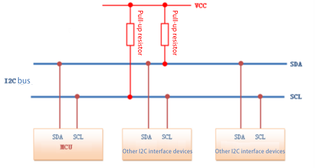
When we design the peripheral circuit of the IIC interface, we usually use the topology diagram with pull-up resistor shown in Figure 1, and its internal structure is the open-drain output shown in Figure 2. The open-drain output level is controlled by an external pull-up and internal logic, allowing the bus to be pulled low and released. The bus open-drain circuit consists of an NMOS transistor, which is turned on and off by a control signal. When the control signal turns on the NMOS transistor, the output is low. When the control signal turns off the NMOS transistor, the output is floating, requiring an external pull-up resistor to output a high level. This structure allows the open-drain gate to flexibly control the bus level while avoiding direct driving of the bus, thus ensuring secure connection and communication between multiple devices. The advantages of using this open-drain output are obvious and are reflected in the following aspects: 1. Short-circuit Prevention If the push-pull configuration is used instead of open-drain, and several devices are connected to the same bus, and an IO on one device outputs a high level while an IO on another device outputs a low level, the VCC and GND connections of these two IOs will short-circuit, causing circuit damage. However, the open-drain configuration eliminates this problem. Regardless of the number of devices connected to the bus, there is no power short-circuit risk. 2. Increase drive capability and reduce power consumption Connecting a pull-up resistor to the drain_output pin allows for level shifting and provides stronger drive capability. This leverages the drive capability of the external circuit to reduce the internal IC drive. When the internal MOSFET of the IC is on, the drive current flows from the external VCC through Rpull-up, the MOSFET, and then to GND. Only a small gate drive current is required within the IC. 3. Use "Wired AND" to determine bus active status Multiple open-drain output pins can be connected to a single line to form an "AND" logic relationship, known as the "wired AND" function. When any one pin goes low, the logic level on the open-drain line becomes 0. This is also the principle used by the I2C bus to determine bus active status. 4. Facilitate output level shifting The transmission level can be changed by varying the pull-up power supply voltage, while the output high level is determined by VDD.
Read More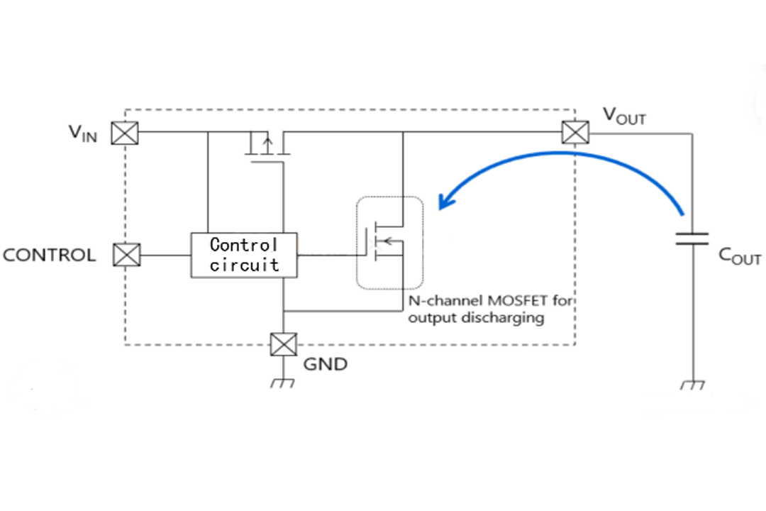
LDOs regulate their output voltage to ensure stable operation under varying load current demands. However, when the load current exceeds the designed range, such as in a short circuit or overload, the excessive current can cause chip overheating or even damage. To address this, overcurrent protection mechanisms have emerged to limit the output current and protect both the LDO and its load. LDOs typically have two overcurrent protection mechanisms: brick-wall current limiting and overcurrent shutdown. 1. Brick-Wall Current Limiting As the name suggests, brick-wall current limiting is a "hard" cutoff mechanism. When the output current exceeds the preset current limit, I_LIMIT, the LDO quickly limits the output current to I_LIMIT. Due to the high load current, the LDO temperature gradually rises. Once the LDO protection temperature is triggered, the LDO output is immediately shut down. The output voltage-current curve resembles a "brick wall" preventing further current increase. For example, the TPS7A16 data sheet lists its brick-wall current limit threshold at 105mA (typical). As can be seen from the output voltage-load current curve in the figure above, when the load current exceeds I_LIMIT and triggers the LDO temperature protection, the output voltage drops sharply. This mechanism is typically implemented through an internal current sensing circuit combined with a temperature protection circuit. The LDO's internal structure includes a current mirror to detect current. When the sensed current exceeds the set reference current, the current limit is triggered, the LDO temperature rises, and when it reaches the protection temperature, the power transistor is turned off, cutting off the output. This indicates that brick-wall current limiting is safer during short-term overloads. Its characteristic is that it can tolerate short-term overloads, but if the overload persists, heat accumulation will trigger thermal shutdown. 2. Foldback Current Limit Foldback current limiting is very similar to standard upper-limit limiting. However, its primary purpose is to limit total power dissipation. This means that as VOUT decreases and VIN remains stable, the output current limit is linearly reduced to keep the output transistor within a safe power dissipation limit. Devices such as the TLV717P incorporate and benefit from foldback current limiting because they are primarily housed in ultra-small packages with higher thermal resistance. The output current limit behavior of the TLV717P is shown in Figure 3. As can be seen, since VIN is specified at VOUT + 0.5V, the maximum allowable power dissipation at 25°C is 150mW. After the current limit is exceeded and VOUT begins to decrease (assuming RLOAD is constant), both IOUT and power dissipation decrease. This adds a slight complexity to non-ohmic devices that consume a constant current and can trigger a latched state where the powered device continues to reduce VOUT and the LDO continues to reduce IOUT. 3. Overcurrent Shutdown Unlike brick-wall current limiting and foldback current limiting, overcurrent shutdown protection utilizes a fast internal shutdown mechanism. The LDO's internal structure incorporates a current mirror to sense current and a comparator to achieve rapid overcurrent output shutdown. When the LDO output current reaches the overcurrent protection level, the LDO shuts down immediately. Therefore, current threshold protection is faster than brick-wall current limiting and foldback current limiting. If the LDO output is loaded with a large capacitive load, the LDO output will experience a large inrush current, potentially triggering the LDO's overcurrent shutdown mechanism and preventing it from starting properly. In this situation, an LDO with overcurrent shutdown should not be selected.
Read More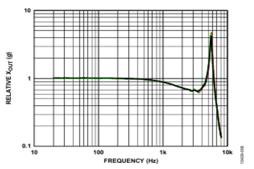
The resonant frequency of the accelerometer chip is a very important performance indicator, which is related to the operating frequency range of the sensor. 1. Definition of resonant frequency The accelerometer sensor itself is also a mechanical structure, so it also has a natural frequency. As shown in the amplitude-frequency curve in Figure 1, when the external vibration frequency is close to the resonant frequency, the sensor will resonate, and the sensitivity of the accelerometer will increase rapidly. The corresponding frequency at this time is the resonant frequency. 2. The influence of resonant frequency on sensor performance The smaller the sensor size, the higher the resonant frequency. The upper limit frequency of the accelerometer depends on the resonant frequency in the amplitude-frequency curve. Generally, the operating frequency range of the accelerometer sensor is less than 1/3 of its own resonant frequency. When the measured vibration frequency is much lower than the resonant frequency, the signal output of the accelerometer is proportional to the measured acceleration. 3. Factors affecting the resonant frequency As mentioned above, if the resonant frequency of the sensor chip is increased, the operating frequency range can be widened, the flat frequency band of the sensor will become wider, the working range will become larger, the accelerometer can be used in more scenarios, and the applicability will be better. But in fact, the increase in resonant frequency is also restricted. According to the following formula, the smaller the mass block, the larger the resonant frequency. Where f0 is the resonant frequency, K is the equivalent stiffness of the accelerometer, and M is the equivalent mass of the sensor. Therefore, the resonant frequency is a hard constraint that determines the available frequency response range of the accelerometer. Reasonable design and application require the operating frequency to be limited to less than 1/3 of the resonant frequency, and in high-precision applications, it needs to be limited to less than 1/5 to ensure linearity and reliability. The frequency response of the ADXL356 shown in Figure 2 has a resonant frequency of approximately 5.5KHz and a 3dB bandwidth of 2.5KHz. In high-precision applications, the cutoff of the low-pass filter is generally set to less than 1KHz.
Read Moreleave a message
Scan to Wechat :