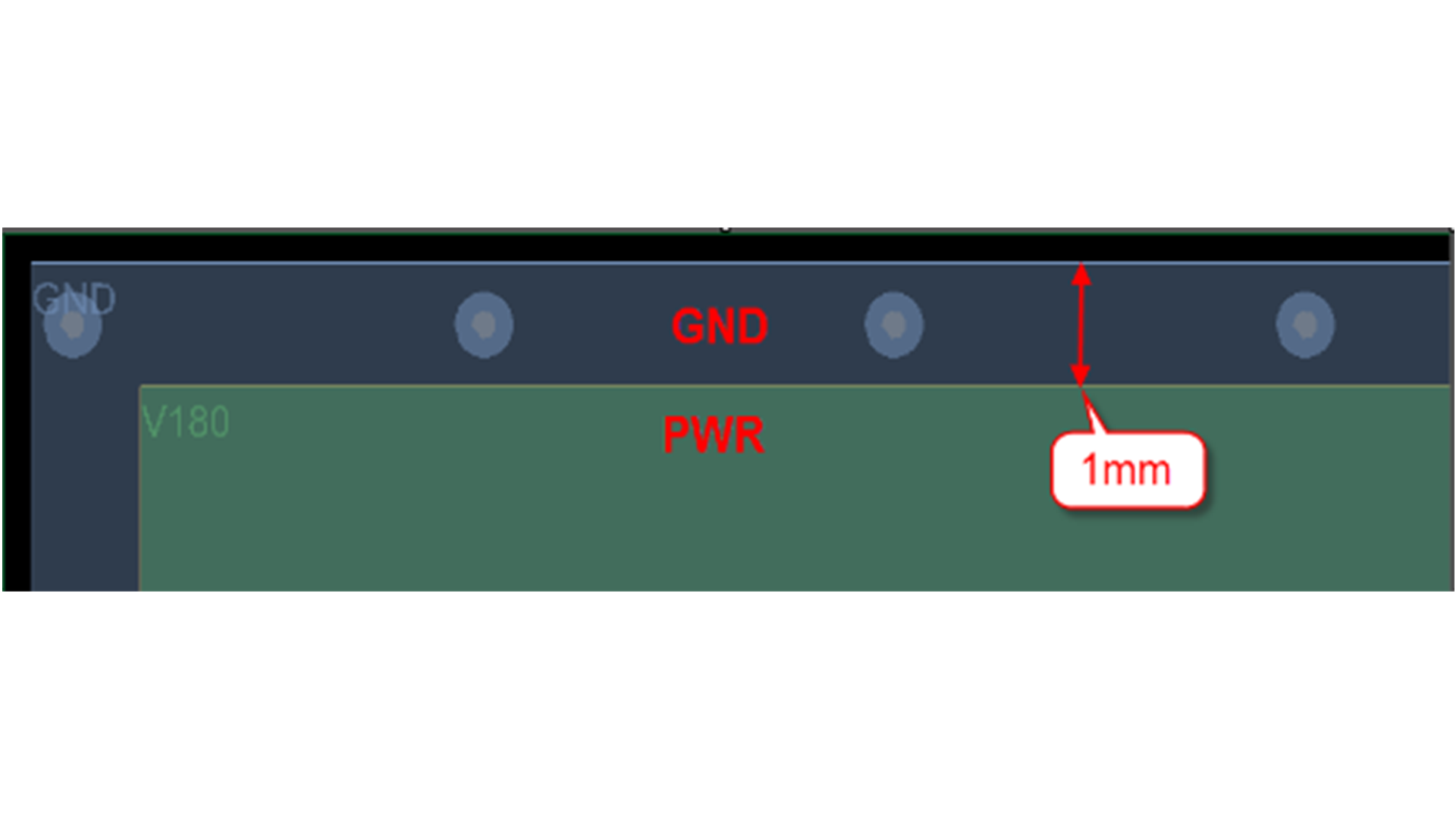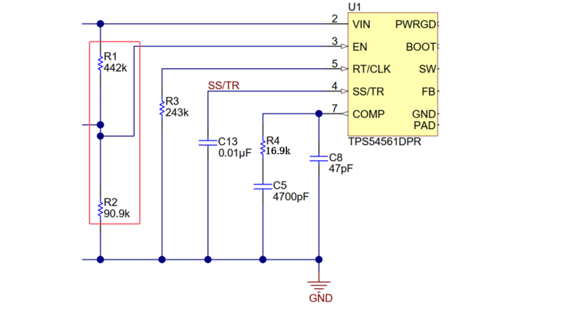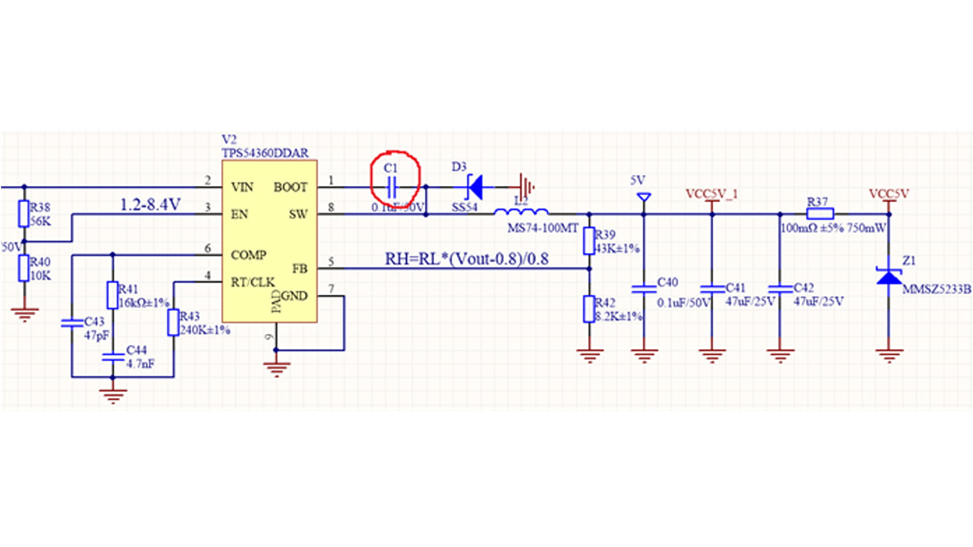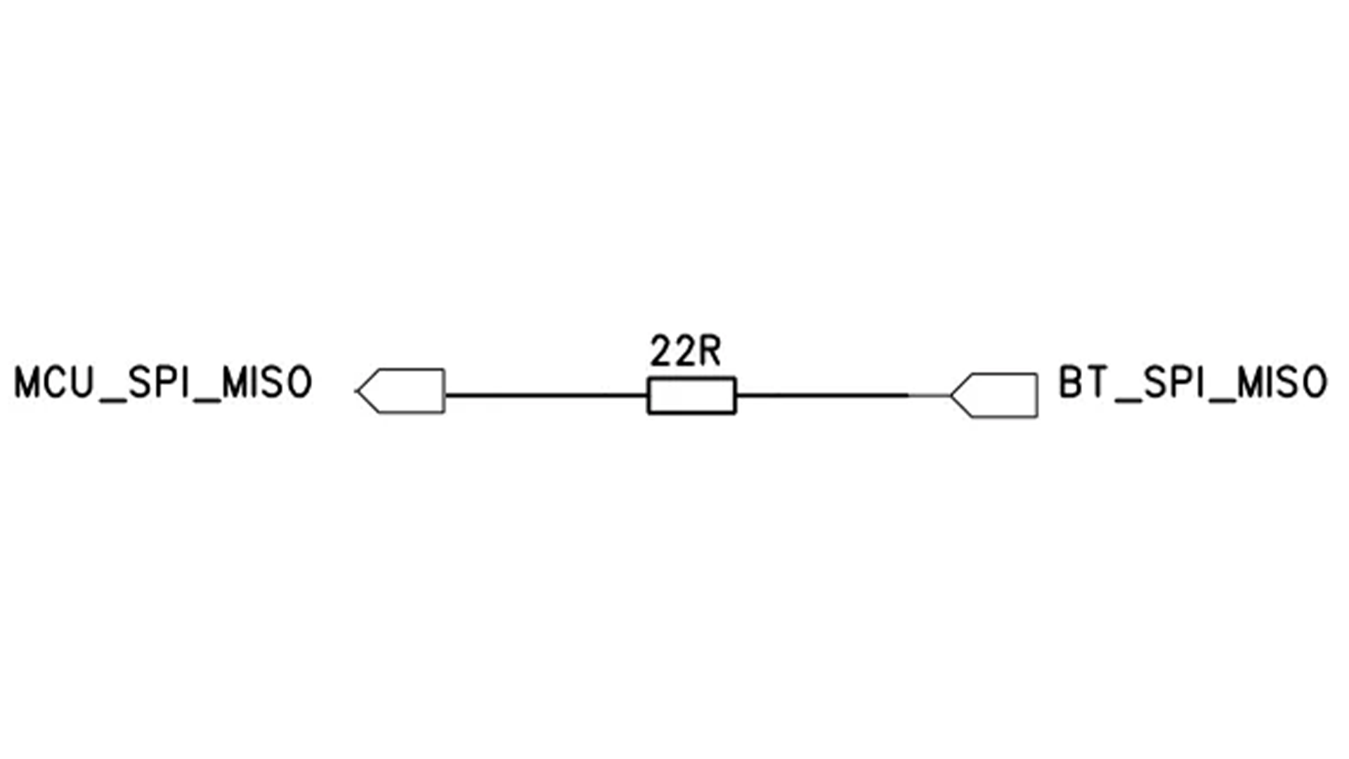
•   When designing the clock circuit diagram for an MCU, if an active crystal oscillator is used as the clock source, a resistor of several tens of ohms is usually added to its output. This resistor primarily serves the following purposes: 1. Impedance Matching When the output impedance of the active crystal oscillator does not match the impedance of the PCB transmission line (usually 50Ω), it can lead to signal reflection, causing overshoot and ringing. By adding a 33Ω resistor in series at the source (forming a 50Ω match with the crystal oscillator's internal resistance of approximately 20Ω), reflected signals can be absorbed, reducing the reflection coefficient. 2. Reducing EMI The output signal of an active crystal oscillator is a square wave signal. The steep edges and the resulting high-frequency ringing generate a large amount of high-frequency noise, which radiates outwards, leading to electromagnetic compatibility (EMC) problems and potentially affecting other parts of the system or failing EMC testing. The series resistor smooths the signal edges, reducing the high-frequency components of the signal, thus effectively reducing electromagnetic radiation (EMI). This is a low-cost and effective EMI suppression measure. 3. Limiting Crystal Oscillator Output Current and Protecting the Output Stage The output driver inside an active crystal oscillator usually has limited capacity. If the input capacitance of the subsequent load is large, or if an accidental short circuit occurs (although rare), a large instantaneous charging and discharging current will be generated at the moment of the square wave transition (charging current i = C * dv/dt). The series resistor can limit this peak current, reducing the burden on the crystal oscillator's internal output stage, providing a certain degree of protection and improving system reliability.

    Read More
  • The function of a TVS (Transient Voltage Suppressor) is to protect electronic circuits from damage caused by transient overvoltages (such as lightning strikes and electrostatic discharge).  It ensures circuit safety by rapidly clamping and diverting surge energy. In TVS protection circuit design, a resistor is usually connected in series, as shown in Figure 1, where a 22Ω resistor is connected in series with both the receiving and transmitting lines of the RS232 communication interface circuit. The TVS is connected in series with the resistor to absorb energy during overvoltage events, protecting the circuit and limiting the current. This configuration ensures that when the circuit is threatened by transient overvoltage, the TVS can quickly intervene and effectively absorb the overvoltage, thus protecting other components in the circuit from damage. At the same time, the series resistor further regulates the current magnitude, preventing the TVS from being damaged by excessive current while absorbing the overvoltage. Figure 1 RS232 communication interface There are generally two ways to connect a TVS with a series resistor: one is to place the resistor after the TVS, as shown in Figure 2, and the other is to connect the resistor before the TVS, as shown in Figure 3. These two methods vary depending on the application scenario. The front connection method can reduce inrush current, while the rear connection method can more effectively perform secondary voltage division and current limiting. Figure 2 Figure 3 In the circuit shown in Figure 2, the TVS device initially absorbs most of the inrush current. Subsequently, any remaining residual voltage or current is divided and current-limited again through resistor R2. This design more effectively protects the downstream load. However, if the impedance of the downstream load is much greater than that of resistor R2, the voltage division and current-limiting effect becomes relatively small, and the role of resistor R2 is relatively weakened.   In the circuit shown in Figure 3, when considering the magnitude of the inrush current, if the surge is small, a resistor of appropriate power can be selected and placed before the TVS. In this way, the resistor will share a small portion of the current, thereby reducing the inrush current IPP. Consequently, the clamping voltage Vc of the TVS will also decrease accordingly, further enhancing the protection effect on the downstream load.

    Read More
  • RS485 is widely used in various fields such as industrial intelligent instruments and communication equipment due to its strong anti-interference ability and low cost. However, industrial environments are complex and subject to severe electromagnetic interference. Non-isolated RS485 systems have the following disadvantages: (1) In outdoor or industrial environments, lightning strikes and power switching can generate transient high-voltage surges, which can easily damage the backend circuit; (2) When multiple devices share the RS485 bus, a fault at one node (such as a short circuit) can cause the entire bus to fail; (3) When the distance between 485 communication nodes is too far (greater than 50 meters), the reference ground of each node is connected to the local ground. When there is a large voltage difference between the grounds at both ends, the ground potential will be superimposed on the signal line as a common-mode voltage, which may exceed the common-mode voltage range that the port can withstand, affecting normal communication, or even damaging the backend circuit; (4) When the ground planes between distant 485 communication nodes are connected using cables (such as 485 shielded cables), the ground wire will form a ground loop with the earth, coupling external common-mode noise and generating ground loop currents, which may cause the entire circuit system to fail. If these unfavorable factors exist, or if safety regulations require electrical isolation between devices to prevent leakage or sparks from causing hazards, an isolated RS485 solution must be considered. An isolated RS485 circuit adds electrical isolation capabilities to the non-isolated circuit, resulting in stronger anti-interference and system stability. Achieving isolation in an RS485 circuit requires the use of isolation devices, such as optocouplers, magnetic isolators, and isolation chips. Optocouplers are the most commonly used isolation devices and are relatively inexpensive. The speed of the optocoupler must meet the baud rate requirements; generally, high-speed optocouplers are used for RS485 electrical isolation, and a DC-DC isolation module is needed to provide independent power to the node. Figure 1 shows a low-cost RS485 electrical isolation solution.

    Read More
  • RS232 (also known as EIA RS-232) is one of the commonly used serial communication interface standards. It uses full-duplex communication and requires three lines: ground, transmit, and receive. RS-232 is only suitable for point-to-point communication between devices. Due to its single-ended signal, it has poor anti-interference capabilities. Therefore, RS232 improves signal anti-interference and increases transmission distance by increasing the voltage level. RS232 uses negative logic levels, with a logic 0 level of [3, 15]V and a logic 1 level of [-15, -3]V. The maximum transmission distance of the RS232 standard is affected by many factors, mainly depending on the transmission rate, cable characteristics, chip driving capability, and signal transmission characteristics. 1. Transmission Rate Transmission distance is inversely proportional to the baud rate. The higher the baud rate, the more severe the signal attenuation and distortion. At 19.2 kbps, the distance usually does not exceed 15 meters. At 9.6 kbps, the distance can reach 30-50 meters. At rates as low as 1.2 kbps, it may reach 300 meters (with other conditions optimized). 2. Cable Characteristics The RS232C standard specifies that the driver is allowed to have a capacitive load of 2500 picofarads. When using a communication cable with a capacitance of 150 picofarads per meter, the maximum communication distance can reach 15 meters. If the capacitance per meter of the cable is reduced, the communication distance can theoretically be increased accordingly. 3. Chip Driving Capability Early chips had weaker driving capabilities, while modern chips (such as MAX232) can support longer distances with driving currents reaching 1mA. 4. Signal Transmission Characteristics • RS232 uses a single-ended signal transmission method, which has problems such as common-ground noise and the inability to effectively suppress common-mode interference, further limiting its transmission distance. Using shielded cables to reduce external electromagnetic interference can also increase the transmission distance. In practical applications, RS232 communication lines are usually used for short-distance communication within 20 meters.

    Read More
  • In industrial applications, to accurately measure temperature values, we typically use a PT100 bridge circuit to sample and convert resistance changes into voltage changes. To obtain different measurement ranges, the sampling resistors are divided into 100 ohms and 50 ohms. Method 1 and Method 2 are the measurement calculation formulas for PT100. The specific differences are as follows: Method 1: (PT100) Reference resistor R3 = 100Ω. This method cannot measure temperatures below zero. The measurement temperature range of Method 1 is >= 0℃. Substitute the values: R1 = R2 = 2000Ω; R3 = 100Ω; R4 = R; Let the measured voltage VT = VTP - VTN as Remove the denominator, Refine expressions Vref is the reference voltage acquired by the AD converter, and VT is the measured voltage. Method 2: (PT100) Reference resistor R3 = 50Ω, measuring resistance offset downwards by 50 ohms, measuring temperature range >=-125℃. Substitute the values: R1 = R2 = 2000Ω; R3 = 50Ω; R4 = R; Let the measured voltage VT = VTP - VTN Remove the denominator, Refine expressions Vref is the reference voltage acquired by the AD converter, and VT is the measured voltage.   Through the calculation process above, we obtained the calculated resistance value of the PT100 by measuring the sampled voltage. To ultimately obtain the relationship between resistance and temperature, typical methods include table lookup and iterative methods.

    Read More
  • In the STM32 reset circuit shown in Figure 1, a switching diode is usually connected in parallel with the resistor terminal of the RC reset circuit. The main function of this diode is to accelerate the release of capacitor charge. Figure 1 STM32 reset circuit Figure 2 Discharge path of STM32 reset circuit In an RC reset circuit, a discharge diode is indispensable, its main function being rapid discharge. When the power is off or there is a momentary power outage due to interference, the charge stored in the capacitor needs to be released through some path to ensure proper reset upon the next power-on. Without a diode, when the power-off interference pulse is narrow, the capacitor discharges through resistor R1, which has a large resistance, resulting in a slow discharge speed. The RC circuit cannot fully discharge at the moment of power failure, and the system cannot automatically reset upon power restoration. The momentary power outage interference can cause the program to stop running normally, leading to program erratic behavior or entering an infinite loop. The addition of a diode provides a rapid discharge path for the capacitor. Due to the diode's very low on-resistance, as shown in the STM32 reset circuit discharge path in Figure 2, the charge in capacitor C1 discharges rapidly through diode D1, ensuring the stability and reliability of the reset circuit. When the power is off, the capacitor discharges rapidly to ground through the diode. When the power is restored, the capacitor has already discharged completely and can immediately begin the charging process, triggering the reset operation. This rapid discharge process ensures that the reset circuit can quickly return to its initial state after a power outage or abnormal power supply.

    Read More
  • When designing switching power supply circuits, we typically calculate the output ripple using the following formula: If the capacitor used is an MLCC (Multi-Layer Ceramic Capacitor), its ESR is negligible due to its very low value. Therefore, based on the input/output voltage, switching frequency, and target ripple, the capacitance can be calculated using the following formula: However, the capacitance value calculated using the above formula resulted in a larger output ripple during actual testing. Why is this? This is because MLCC (Multi-Layer Ceramic Capacitors) have a DC bias characteristic: applying a DC voltage to the capacitor reduces its capacitance.   Figure 1 below shows the DC bias characteristic of Murata's 22uF/10V capacitor. Figure 1 As can be seen, when a DC voltage of 5V is applied to the capacitor, its capacitance is reduced to approximately 50% of its initial value. The DC bias characteristic of MLCC capacitors is very pronounced; the larger the capacitance, the faster the capacitance decreases with increasing voltage, which must be considered in circuit design. Generally, the DC bias characteristics of MLCC capacitors have the following characteristics:   ① The larger the capacitance, the more pronounced the bias characteristic; the capacitance decreases more with increasing voltage.   ② For capacitors of the same capacitance but different voltage ratings, the capacitance decreases approximately the same under the same voltage (there is no capacitor with a high voltage rating that decreases less).   ③ For capacitors of the same capacitance and voltage rating, the larger the package, the slower the capacitance decreases.   The capacitance decay of MLCCs is an objective reality. Design should be based on the capacitance under the actual bias voltage, not the nominal capacitance. For example, if a circuit requires a 10uF capacitor, and an X7R type MLCC (10V rated) is selected, with an actual bias voltage of 5V (at which point the capacitance decays by approximately 50%), then two capacitors with a nominal capacitance of 10uF should be connected in parallel to ensure that the actual capacitance meets the requirement.

    Read More
  • In a step-down switching converter, the theoretical peak current that the power inductor can withstand is IL,PK=(1+r/2)×IOUT. This is the basis for the minimum value of the rated current or saturation current of the power inductor. The actual selection value needs to be greater than the theoretical value of the peak current. Once the inductance value and other conditions of the power inductor are determined, the actual peak current of the inductor is Ipeak = Iout,max + ∆I_L/2 (where ∆I_L is the actual ripple current on the inductor after the inductance value is determined). The formula for calculating the minimum value of the power inductor in a BUCK circuit is as follows: Where VIN,MAX is the maximum input voltage that the BUCK circuit needs to support, VOUT is the typical output voltage, FSW is the switching frequency, IOUT,MAX is the maximum load current that needs to be supported, and r is the ripple current coefficient, which is typically set to 0.3~0.5. The above formula is the basis for determining the minimum power inductance value in the BUCK buck converter. The actual value must not be less than the theoretically calculated value; otherwise, the actual ripple current and other parameters in the circuit will not meet the target values ​​in the design requirements. By transforming the above formula, we obtain the formula for calculating the minimum power inductance value, as shown below: Therefore, it can be seen that the input voltage VIN is directly proportional to the inductance L; the larger the input voltage (the maximum input voltage that needs to be supported is VIN,MAX), the larger the required inductance. If the designed BUCK circuit only needs to support the typical input voltage value VIN,TYP, that is, the input voltage is a fixed value, then the calculation of the minimum power inductance mentioned above can also use VIN,TYP.

    Read More
  • Figure 1. Non-synchronous BUCK converter topology Figure 1 shows the topology of an asynchronous BUCK converter. Asynchronous BUCK converter chips typically integrate only the high-side MOSFET internally. A freewheeling diode needs to be installed between the SW pin and GND as the freewheeling path for the power inductor when the high-side MOSFET is turned off. The selection of the freewheeling diode must meet at least the following two hard criteria (1)(2) and two optimization criteria (3)(4): (1) The reverse operating voltage VRRM of the freewheeling diode must be equal to or greater than the maximum input voltage VIN(max). (2) The forward conduction current IF(AV) of the freewheeling diode must not be less than Iout(max)*(1-D), where D is the duty cycle of the buck converter, and Iout(max) is the maximum load current that the buck converter can support. For a more stringent selection of the freewheeling diode's overcurrent capability, it can be selected to be greater than or equal to the peak current on the inductor IOUT+(ΔIL)/2. (3) The smaller the forward voltage drop VF, the smaller the power loss caused by this parameter, and the higher the power efficiency. (4) The faster the switching speed from the on state to the off state (the smaller the reverse recovery time trr), the smaller the reverse recovery loss, and the higher the power efficiency, the better. Schottky barrier diodes (SBDs) are ideal choices for freewheeling diodes due to their small forward voltage drop and fast reverse recovery time (typically tens of nanoseconds or even a few nanoseconds), reducing power losses in the freewheeling diode. To design a step-down DC-DC converter with a DC input voltage range of 9-36V, a typical input voltage of 12V, an output voltage of 5V, and a maximum load capacity of 5A, a Schottky diode with a reverse operating voltage of 40V and a forward current greater than 5A is selected because its maximum input voltage is 36V. As shown in Figure 2, the SS54 Schottky diode has a reverse operating voltage of 40V, an average rectified current of 5A, and a maximum forward voltage drop of 0.55V at a forward current of 5.0A, meeting the circuit requirements. Figure 2 Electrical parameters of SS54 Schottky diode When the input voltage is a typical 12V, the duty cycle is a typical 5/12, and the average current flowing through the freewheeling diode is 5.0A*(1-5/12)=2.917A. When the input voltage is the maximum value of 36V, the duty cycle is a minimum of 5/36, and the maximum average current flowing through the freewheeling diode is 5.0A*(1-5/36)=4.3A. As shown in Figure 3, D3 (SS54) in the TPS54360DDAR circuit design example is the selected freewheeling diode. Figure 3. TPS54360DDAR circuit design example  

    Read More
  • The previous article mentioned that in order to suppress the influence of high-frequency noise, the 4-20mA current sampling circuit needs to add an RC low-pass filter before ADC sampling. The RC low-pass filter circuit shown in Figure 1 is adopted, where R2 is 1.6K and C1 is 0.1uF. Then the cutoff frequency fc is approximately 1KHz. Figure 1 RC low-pass filter The following analysis examines its noise suppression capability through practical calculations, using a 200Hz in-band signal and a 5kHz out-of-band noise signal as examples to calculate its amplitude-frequency response. The output of a typical resistor divider is shown in Figure 2. Figure 2 Resistor voltage divider output The RC filter uses an equivalent structure, replacing R2 with a capacitor. First, we replace R2 with the capacitive reactance (XC) of the capacitor, obtaining the output expression of the RC voltage divider as shown in Figure 3:   Figure 3. Resistor-capacitor voltage divider output The expression for the capacitive reactance of the capacitor is as follows: Figure 4. Expression for capacitive reactance of a capacitor In the design example above, R ≈ 1600Ω and C = 100nF. We assume the amplitude of VIN is 1V, and calculate the amplitude of VOUT using a sine wave frequency of 200Hz (Figure 5): Figure 5 The calculation results in Figure 5 show that the amplitude of the 200Hz signal remains essentially unchanged, which is consistent with the expectation of maintaining the signal amplitude without attenuation while suppressing noise. Next, let's see how the filter successfully attenuates the 5kHz noise component (Figure 6). Figure 6 The calculation results in Figure 6 show that the noise amplitude is only about 20% of its original value, which demonstrates that the suppression effect on out-of-band noise is significant.

    Read More
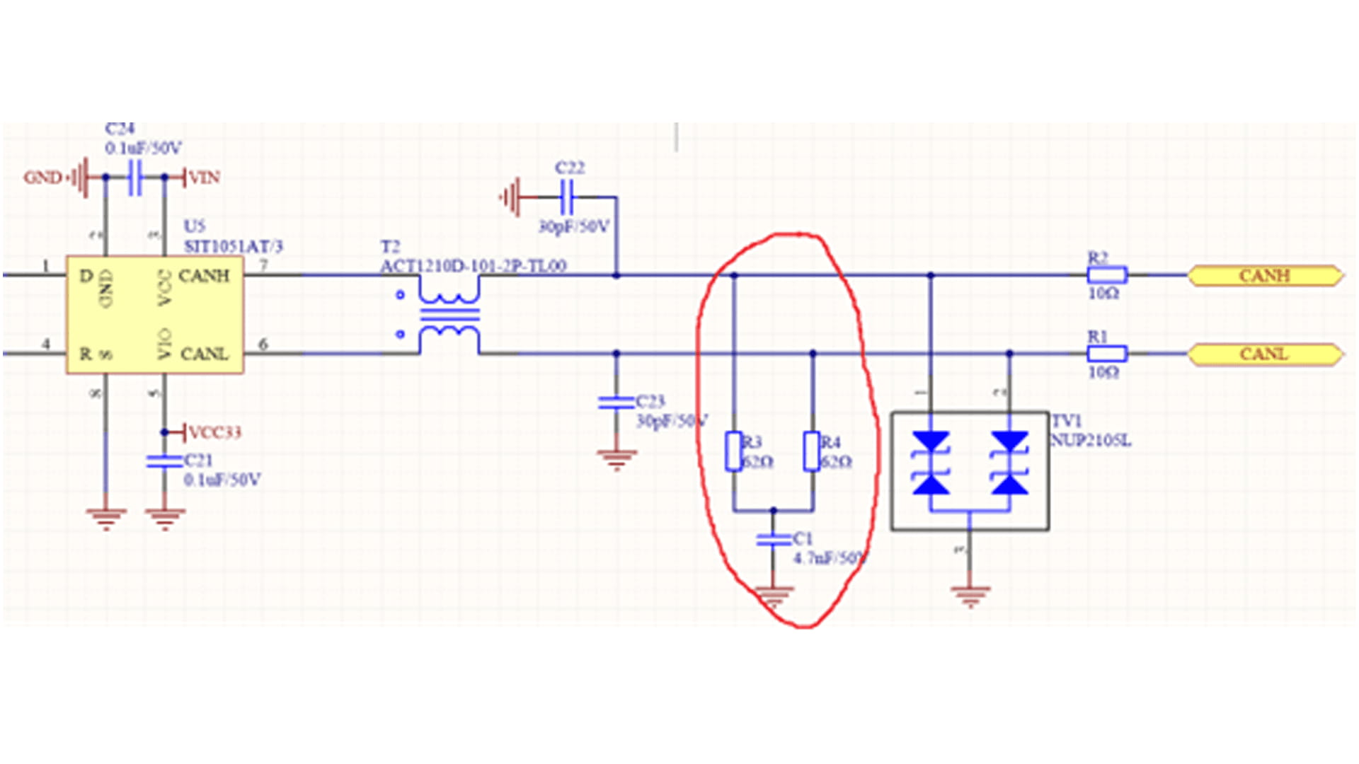
  • We often see the design circuit shown in the figure below in CAN communication: the CAN terminal resistor does not directly use 120 ohms. Instead, a grounded capacitor is added between two 62Ω resistors to "split" the terminal resistor into two parts, which is the split termination method. Figure 1 CAN bus interface circuit This connection method is actually quite sophisticated; it effectively reduces external interference on the differential signal. The CAN bus transmits differential signals, which are generally highly resistant to common-mode interference. However, for high-reliability design, the CAN bus must withstand a variety of harsh environments. High-amplitude common-mode spike interference on the bus can damage the ground-connected circuitry within the CAN transceiver, necessitating interference suppression. The simplest and most effective method for suppressing this interference is to use an RC low-pass filter. This involves splitting the 120Ω termination resistor into two 62Ω resistors connected in series, with a small capacitor connected to ground between the two resistors. This creates an RC low-pass filter at each of the two differential transmission ports, CANH/CANL, on the CAN bus.   The cutoff frequency of an RC low-pass filter is Fc = 1/(2πRC), so C = 1/(2πRFc). This means that the size of the capacitor is related to the signal transmission cutoff frequency. The choice of capacitor is typically determined by the baud rate. For a 500kHz baud rate, we choose a cutoff frequency of 500kHz. The capacitance calculation formula is: C = 1/(2πRFc) = 1/(2π*500000*62) = 5.13nF. A capacitor of 4.7nF, which is close to the commonly used value, is sufficient. The CAN bus uses split termination to more effectively filter out high-frequency common-mode noise, improving communication stability in complex industrial environments.    

    Read More
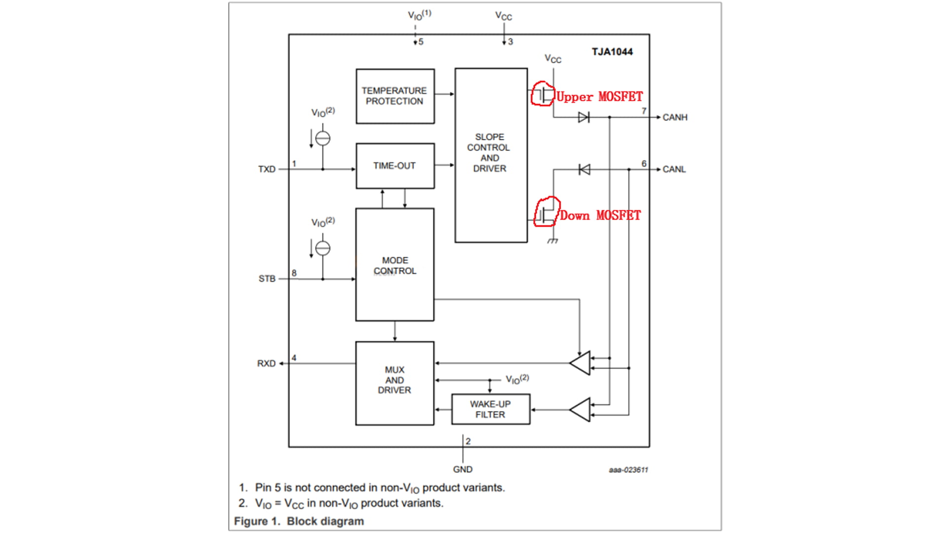
  • In the actual use of the CAN bus, as shown in Figure 1, a 120Ω resistor needs to be connected at both ends of the bus. So what is the basis for using a 120Ω resistor? Figure 1 Below we take the internal architecture diagram of TJA1044 as an example for analysis. Figure 2 The CAN bus's characteristic is that dominant represents 0, and recessive represents 1. When the bus is recessive, both the upper and lower transistors Q1 and Q2 within the TJA1044 are turned off, leaving CANH and CANL inactive with a voltage difference of 0V. When the bus is dominant, both the upper and lower transistors Q1 and Q2 within the TJA1044 are turned on, creating a voltage difference between CANH and CANL. If there is no load on the bus and the bus is recessive, the bus's differential resistance will be very large, causing even minimal external energy to cause the bus to become dominant. This is primarily because the minimum threshold voltage for dominant in typical transceivers is only around 500mV. Therefore, to improve the bus's immunity to interference, a termination resistor is required. However, this resistor should be kept as low as possible (and also to avoid excessive current).   In addition, parasitic capacitance on the bus must also be considered. When the bus is dominant, the capacitor charges, and when it is recessive, the capacitor discharges. If the bus does not have any parallel resistors, the bus can only discharge through the transceivers at both ends. This affects the transition time between the two states (recessive and dominant), resulting in waveform anomalies (climbing), as shown in Figure 3. When a signal encounters an impedance discontinuity in a high-speed transmission path, it causes signal reflections, which we call impedance discontinuities. Adding terminal resistors can eliminate or reduce the impact of these signal reflections. The terminal resistors absorb signal energy, preventing it from dispersing on the bus. So why 120Ω? In fact, the ISO 11898-2 standard clearly defines 120Ω as the most reasonable resistance value determined through extensive experimental testing. Figure 3 If you want to verify how large the terminal resistance of the bus is required in an actual project, you can test it using the method shown in Figure 4 below. Figure 4 Connect an adjustable resistor in parallel to the bus and adjust it until the square wave waveform remains undistorted. When selecting the terminal resistor power, the short-circuit condition of the interface must be taken into account. This means that in the event of a short circuit, the short-circuit current will flow directly from CANH to CANL. However, the current that a typical CAN transceiver can withstand is only tens of mA (due to internal current limiting measures within the transceiver). For example, the TJA1044 only handles 50 mA. Based on P = I² * R, we get 50 mA * 50 mA * 120 Ω = 0.3 W. Therefore, the resistor power is selected to be 0.25 W, which is the common 1206 package.  

    Read More
Prex
1 2 3 4
Next

leave a message

leave a message
If you are interested in our products and want to know more details,please leave a message here,we will reply you as soon as we can.

Home

Products

whatsApp

Contact

Shopping Cart
item.name
[[ item.product_name ]]
* [[ item.qty ]]
Your Cart Is Empty!