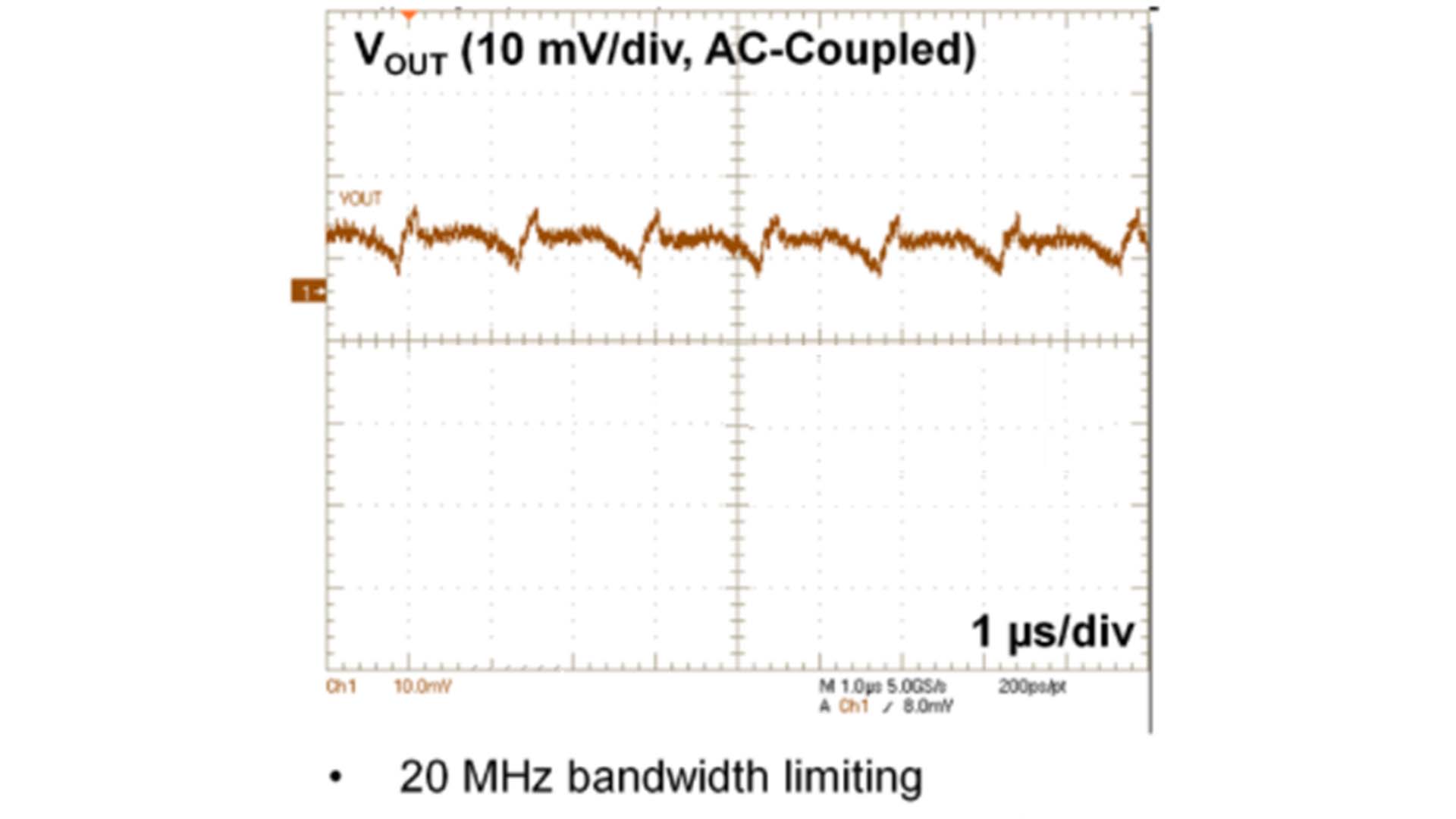
• Load regulation refers to the change in output voltage when the load current is adjusted from a minimum value to a maximum value while the input voltage remains unchanged, that is, the ability to maintain a stable output voltage when the load current changes steadily. It is a steady-state indicator. The output load regulation indicator is usually expressed in mV in the LDO specification. From the definition, it can be seen that the smaller the load regulation, the better. When the load current changes suddenly, the smaller the output voltage change caused, the better the LDO performance. For LDO power supply, its output voltage is different under different load current conditions. For example, assuming that the load current of a certain LDO changes from 10mA to 300mA, the output voltage changes from 3.3V to 3.28V, that is, when the load current is 10mA, the output voltage is 3.3V; when the load current is 300mA, the output voltage is 3.28V. If the load regulation is expressed in mV, it is 3.3V-3.28V=0.02V=20mV. This means that when the load current is within 10mA~300mA, the maximum output voltage change does not exceed 20mV. Output capacitors of different sizes have different load regulation rates. The larger the output capacitor, the more stable the output voltage will be. In the figure below, when the green Iout suddenly rises, the LDO output has an undershoot, which is the load regulation rate.

    Read More
  • Power Supply Rejection Ratio (PSRR) refers to the ratio of the input ripple voltage to the output ripple voltage, in decibels (dB), and its expression is: The significance of PSRR lies in quantifying the degree of transmission of changes in the power input to the output. For example, if the PSRR of a certain circuit is 60dB, then for every 1V change in the power supply input voltage, the output will only fluctuate by 1mV. This indicator is particularly important in analog circuits (such as op amps, voltage regulators) because power supply noise can directly lead to signal distortion or system performance degradation. The factors affecting the PSRR of the LDO power supply are not only related to the ripple frequency, but also to the load current, input and output voltage difference, and output capacitor capacitance value. Specifically, it is reflected in: the smaller the voltage drop, the larger the load current, the higher the frequency, and the smaller the output capacitor, the lower the PSRR. Therefore, when a high common mode rejection ratio is required, it is necessary to appropriately increase the voltage difference, increase the output capacitor and reduce the load current. Figure 1 shows a schematic diagram of the relationship between the PSRR and frequency of the AP2210 ultra-low dropout difference power supply chip. From the diagram, it can be seen that its PSRR can reach 75dB at low frequency. Picture 1  PSRR vs Frequency Usually, the LDO power supply has a high PSRR, so the output ripple is low. Therefore, when designing the power supply circuit of the sensor, especially the sensor with analog output, in order to ensure the accuracy of the sensor, a low-noise and small ripple LDO is usually used to power the sensor. The output ripple of the switching power supply is large and is greatly affected by the load size. In terms of efficiency, the switching power supply is higher than that of LDO and has a smaller heat generation. Therefore, the switching power supply is generally used in combination with LDO, and the high power supply suppression ratio of LDO is used to suppress the output ripple of the switching power supply.

    Read More
  • In order to prevent the power supply user from accidentally connecting the input power line incorrectly and causing the power supply to burn out, an anti-reverse connection circuit is generally required at the power supply input end. At the same time, in order to ensure that the input voltage is within a safe range, the input voltage also needs to be protected against overvoltage cutoff. The circuit shown in Figure 1 realizes the integrated function of anti-reverse connection and overvoltage protection. Its overvoltage protection function is analyzed as follows: When Vin is in the normal input voltage range, the voltage regulator Z1 does not reversely break down, the current of R2 and R3 is basically 0, the Vbe of the transistor P1 is 0, that is, the PNP transistor is not turned on, and the Vgs of the PMOS tube Q1 is determined by the voltage divider of resistors R4 and R5. Vgs is greater than the conduction threshold, and the PMOS tube is turned on, that is, the power supply works normally; when the Vin input is greater than the normal input voltage, at this time Vin>Vbr, the voltage regulator is broken down, the PNP transistor Q1 is turned on, VCE≈0, that is, the Vgs of the PMOS tube is ≈0, and the PMOS tube is turned off, that is, overvoltage protection is achieved. Its reverse connection protection function is analyzed as follows: the input reverse connection protection is realized by NMOS tube Q2. When the positive pole of the power supply is input from Vin, the gate voltage Vgs of NMOS tube Q2 is high. At this time, Q2 is turned on, Q1, load RL and Q2 form a loop, and the circuit works normally; when the positive pole of the power supply is reversed from the negative terminal below, Q2 is cut off, the entire loop is disconnected and the circuit does not work, thereby playing a role in reverse connection protection.

    Read More
  • In order to prevent the power supply user from accidentally connecting the input power line incorrectly and causing the power supply to burn out, an anti-reverse connection circuit is generally required at the power supply input end. At the same time, in order to ensure that the input voltage is within a safe range, the input voltage also needs to be protected against overvoltage cutoff. The circuit shown in Figure 1 realizes the integrated function of anti-reverse connection and overvoltage protection. Its overvoltage protection function is analyzed as follows: When Vin is in the normal input voltage range, the voltage regulator Z1 does not reversely break down, the current of R2 and R3 is basically 0, the Vbe of the transistor P1 is 0, that is, the PNP transistor is not turned on, and the Vgs of the PMOS tube Q1 is determined by the voltage divider of resistors R4 and R5. Vgs is greater than the conduction threshold, and the PMOS tube is turned on, that is, the power supply works normally; when the Vin input is greater than the normal input voltage, at this time Vin>Vbr, the voltage regulator is broken down, the PNP transistor Q1 is turned on, VCE≈0, that is, the Vgs of the PMOS tube is ≈0, and the PMOS tube is turned off, that is, overvoltage protection is achieved. Its reverse connection protection function is analyzed as follows: the input reverse connection protection is realized by NMOS tube Q2. When the positive pole of the power supply is input from Vin, the gate voltage Vgs of NMOS tube Q2 is high. At this time, Q2 is turned on, Q1, load RL and Q2 form a loop, and the circuit works normally; when the positive pole of the power supply is reversed from the negative terminal below, Q2 is cut off, the entire loop is disconnected and the circuit does not work, thereby playing a role in reverse connection protection.  

    Read More
  • According to the topology of the two-wire circuit, the power current is modulated by the sensor and then returns to the signal acquisition circuit. If the power output part does not undergo any processing, once the sensor is short-circuited or the end user operates improperly causing a short circuit, the power is very likely to be damaged or cause damage to the signal acquisition circuit. To avoid this situation, a current-limiting circuit needs to be added to the circuit that provides 24V power to the sensor to limit the current within a safe range (for example, below 30mA), avoiding catastrophic failures. The following presents the current-limiting protection circuit for providing 24V power to the sensor when designing the 4-20mA interface acquisition circuit.   When the current is less than the limiting current Imax, the voltage drop across resistor R1 is less than the Vbe conduction voltage of transistor P1. Resistors R3 and R4 divide the voltage, creating a sufficient voltage difference between the source and gate of the field-effect transistor Q1. At this point, transistor P1 is cut off and transistor Q1 conducts. The circuit is in a normal operating state. When the current increases to be greater than the limiting current Imax, the voltage drop across resistor R1 is greater than the Vbe conduction voltage of transistor P1. At this time, transistor P1 is in the conducting state. The input voltage is directly applied to the gate of the field-effect transistor Q1. At this point, the voltages at the source and gate of the field-effect transistor Q1 are approximately equal, causing the field-effect transistor Q1 to be cut off and disconnecting the circuit, putting the circuit in a protective state. This avoids excessive current damage to the load. Because the Vbe conduction voltage of MMBT2907A is approximately 0.7V, and from Vbe/R1 = 25mA, it can be known that the limiting current is approximately 25mA. If the limiting current needs to be adjusted, simply adjusting the resistance value of resistor R1 is sufficient.

    Read More
  • The main reason for choosing dual power supplies for sensors is to meet the requirements of signal integrity, circuit operating conditions, and measurement accuracy. This includes the following aspects: 1. Handling bidirectional signals (AC signals) Some sensors (such as vibration, sound, and acceleration sensors) output signals that are bidirectional, meaning they fluctuate above and below the zero reference point (positive and negative voltages). If only a single power supply is used, the negative half-cycle signal will be truncated, resulting in distortion. At this time, using positive and negative power supplies (such as ±5V, ±12V) to provide symmetrical voltages enables the signal to fluctuate centered at 0V, retaining the complete information of the positive and negative halves to avoid signal distortion. 2. Internal circuit operation requirements Many sensors integrate operational amplifiers or analog circuits for signal amplification or processing within their internal circuits. These devices require positive and negative power supplies to achieve: Simplified circuit design: In a single power supply system, when processing AC signals, a "virtual ground" needs to be set, which introduces additional noise and design complexity. While positive and negative power supplies naturally use "ground" (0V) as the reference point, without the need for additional bias circuits, this simplifies the design and reduces noise. Maximizing dynamic range: Many high-performance sensors and operational amplifiers require dual power supplies to fully utilize their input/output range, avoid non-linear distortion, and improve the linearity and dynamic range of the system. 3. Anti-interference and noise suppression The dual power supply design can reduce common-mode noise interference. Common-mode noise refers to the voltage difference between two signal lines to ground. Using positive and negative power supplies can effectively reduce this voltage difference, thereby reducing common-mode noise interference, especially in industrial environments, symmetrical power supply helps to improve the signal's signal-to-noise ratio.

    Read More
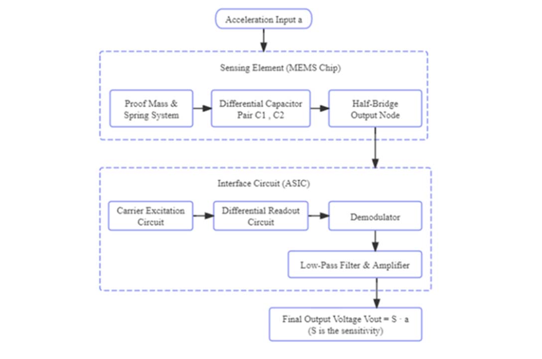
  • 1. Working Principle and Types of Acceleration Sensors An acceleration sensor is a common type of sensor that can measure the acceleration and tilt angle of objects, and is widely used in industries, healthcare, sports, and other fields. Acceleration sensors typically consist of sensing elements, signal processing circuits, and interface circuits, and can sense the acceleration of an object or detect changes in the motion state, converting these data into electrical signals for output. Currently, the market offers two main types of acceleration sensors: analog sensors and digital sensors.The characteristic of acceleration digital sensors is their ease of integration with digital systems. However, sometimes to achieve higher accuracy, lower noise, and to meet different dynamic response requirements, while also controlling costs, we tend to prefer analog output acceleration sensors.Figure 1 shows the processing flow of the signal from a typical analog output accelerometer. Generally, to improve integration and reduce costs, the ADC sampling and digital filtering processing are integrated into the MCU or DSP internally.     2. Design of the Pre-ADC Anti-aliasing Low-pass Filter Adding an anti-aliasing low-pass filter at the front end of the ADC (analog-to-digital converter) is a crucial design in the signal sampling system. According to the Nyquist sampling theorem, the ADC sampling frequency fs must be at least twice the highest frequency fmax of the signal (i.e., fs ≥ 2fmax) to accurately reproduce the original signal without distortion. If the input signal contains components with frequencies exceeding fs/2 (referred to as the Nyquist frequency), these high-frequency components will be "folded" into the low-frequency range, forming false signals (aliasing). Aliasing permanently contaminates the useful signal and cannot be eliminated through subsequent processing. The actual signal may contain noise or useless high-frequency components (such as electromagnetic interference, harmonics), which may exceed fs/2, and even if the input signal itself has a limited bandwidth, the sampling process of the ADC (especially discretization) will introduce quantization noise. The anti-aliasing low-pass filter can reduce the impact of high-frequency noise. The anti-aliasing low-pass filter is actually an RC (resistor-capacitor) low-pass filter, and its cutoff frequency fc is usually set slightly lower than fs/2 but slightly higher than the effective bandwidth of the signal (such as the bandwidth of an accelerometer of 100 Hz, fc is selected as 150 Hz), ensuring that only signals with frequencies below the Nyquist frequency pass through. If the ADC sampling clock frequency is 2 KHz, then the cutoff frequency fc should be set not higher than 1 KHz. The formula for calculating the cutoff frequency fc is fc = 1/(2π×R×C). Using the anti-aliasing low-pass filter to reduce background noise and thereby improve the resolution of the accelerometer. Generally, in the design, the bandwidth is limited to the lowest frequency required by the application to maximize the resolution and dynamic range of the accelerometer.In practical use, if ADI's ADXL103 or ADXL203 is used, the internal low-pass filter is already integrated. The cutoff frequency (-3dB point) is determined by the external capacitor C connected to the output terminal, and only by connecting a capacitor in parallel to the output pin and forming a low-pass filter with the internal output resistor can the anti-aliasing and noise suppression functions be achieved. The actual application circuit is shown in Figure 2, and its corresponding fc = 5 µF/C.     3. Digital Filtering The analog signal passes through an anti-aliasing low-pass filter and is sent to the ADC module. Under the drive of the sampling clock, a continuous data stream is generated. At this time, the data inevitably still contains noise. To filter out the noise, digital filtering technology needs to be adopted to process the obtained data. Compared with analog filters, digital filters usually have more stable frequency responses, can precisely suppress out-of-band signals, have good repeatability, and can be implemented either in pure software or by using hardware acceleration of FIR (Finite Impulse Response) or IIR (Infinite Impulse Response) filters. Digital filtering can be either purely software-based or implemented using hardware acceleration of FIR or IIR.Due to the high order of FIR filters, they consume more computing resources and are more suitable for running on DSP or high-performance MCUs. Their difference equation expression is shown in the following figure.    For a 120th-order low-pass FIR filter using a Kaiser window, the stopband attenuation usually reaches over 60dB. Compared to IIR filters, FIR filters have a wider transition band and larger group delay, and their real-time response is not as fast as IIR filters.If the computing resources are limited on an embedded platform or to obtain a steeper transition band, IIR filters can also be used. Compared to FIR filters, IIR filters have higher computational efficiency (can achieve high performance with lower orders), have nonlinear phase changes, and are acceptable for accelerometers, but they may be unstable. The pole positions need to be carefully optimized. The general expression of the difference equation for IIR filters is as shown in the following figure.    A 4th-order elliptic IIR low-pass digital filter usually can achieve a stopband attenuation of over 60dB when the passband ripple is 0.5dB.Sometimes, in order to obtain a smooth output result, the output data within a certain window of the aforementioned filter is subjected to recursive average filtering to reduce the influence of noise. Given a signal sequence x[n] containing N samples, where n is the index of the sample (from 0 to N-1). Moving average filtering is performed by sliding a fixed-length window of length M over the signal sequence and calculating the average of the samples within the window. For each position k of the sliding window, the filtered output y[k] can be calculated using the following formula:   The size M of the sliding window determines the degree of smoothing. A larger window can more effectively smooth the signal, but it may result in a delayed response; a smaller window can respond to changes in the signal more quickly, but the smoothing effect may be poorer. Usually, when the ADC sampling clock is 2000Hz, M is set to 10.

    Read More
  • The voltage output type sensor typically outputs a voltage range of 0-5V or 0-10V. If we choose not to use an external ADC conversion chip due to cost considerations but instead sample the ADC module within the MCU chip, but as the voltage range of the AD acquisition in STM32 is 0-3.3V, in this case, we need the sampling circuit as shown in the figure below. In the figure, R1 and R2 form a resistor voltage divider circuit, which converts the input voltage ranging from 0 to 5V into a voltage range of approximately 0 to 3V. The subsequent rail-to-rail operational amplifier voltage follower plays the role of impedance matching, isolating the sensor from the ADC sampling module and reducing signal attenuation. To prevent damage to the subsequent ADC module circuit caused by overvoltage and negative voltage, clamp protection diodes are added to the power supply and ground respectively, ensuring that the input voltage of the ADC module is always within the range of -0.7V to 3.3V + 0.7V. At the same time, to suppress the influence of high-frequency noise, an RC low-pass filter needs to be added before ADC sampling. The cutoff frequency of the low-pass filter should be selected according to the bandwidth of the signal. For example, if the signal bandwidth is 100Hz, the cutoff frequency can be set to 100Hz or slightly higher, such as 1kHz. If R2 is 1.5K and C1 is 100nF, then the cutoff frequency fc is approximately equal to 1KHz.  

    Read More
  • If the communication between the sensor module and the user system is carried out using UART, SPI or IO methods, generally, the interface voltage level of the sensor module is 3.3V, and the voltage level of the user system is also 3.3V. Usually, a direct connection method is feasible. However, if the interface voltage level of the user system is 1.8V or 5V, when the module interacts with the single-chip microcomputer system for data exchange, due to the mismatch of the voltage levels of the two communicating parties, it may lead to communication failure, current backflow, abnormal power consumption, voltage abnormality and other problems. This article will introduce several common level matching methods, and users can choose specifically according to the actual situation. 1. Use level conversion chips Supply the two required conversion power supplies to the two sides of the conversion chip, and then connect the required input and output signals of the conversion to the input and output of the chip. All conversion parts are completed by the chip internally. The following figure shows the level conversion circuit using SN74LVC2T45DCTR. The advantages of this scheme are that it is very fast, has strong driving capability, and is easy to use. The disadvantages are that the cost is relatively high. 2. Conversion of levels using MOSFETs or transistors As shown in the figure below, this is a bidirectional level conversion circuit. First, let's analyze the situation where data is sent from 3.3V to 5V. When the UART1_TX terminal is at a high voltage, the MOSFET Q1 is in the cut-off state, and the UART2_RX terminal is pulled up to its power supply voltage. When the UART1_TX terminal is at a low voltage, the MOSFET Q1 conducts, and the UART2_RX terminal is pulled down to a low voltage level by Q1, completing the level conversion. Second, let's analyze the situation where data is sent from 5V to 3.3V. When the UART2_TX terminal is at a high voltage, both the MOSFET Q2 and the body diode are in the cut-off state, and the UART1_RX is pulled up to a high voltage by R3. When the UART2_TX outputs a low voltage, the MOSFET does not conduct, but the body diode of the MOSFET pulls the UART1_RX down to a low voltage level. At this point, Vgs is greater than the turn-on voltage, and the MOSFET conducts, further lowering the voltage of UART1_RX. MOSFETs can also be replaced with transistors. The advantage of this solution is its low cost, while the disadvantage is that the baud rate of the data generally cannot exceed 400 kbps. 3. Using resistors for voltage division to convert levels This solution only uses one type of component - resistors, as shown in the figure below. When the 3.3V level module sends data to the right, it only passes through the current-limiting resistor, and the level at the receiving end of the client is within the range. When the 5V level client sends data to the left, it uses two resistors for voltage division, and the voltage at the receiving end on the left is 5V * 2K / (1K + 2K) ≈ 3.3V. The advantage of this solution is that it has extremely low cost and is convenient for PCB board layout. The disadvantage is that it has weak driving capability and cannot achieve very high speed. Generally, the baud rate applied in this way does not exceed 100 kbps.

    Read More
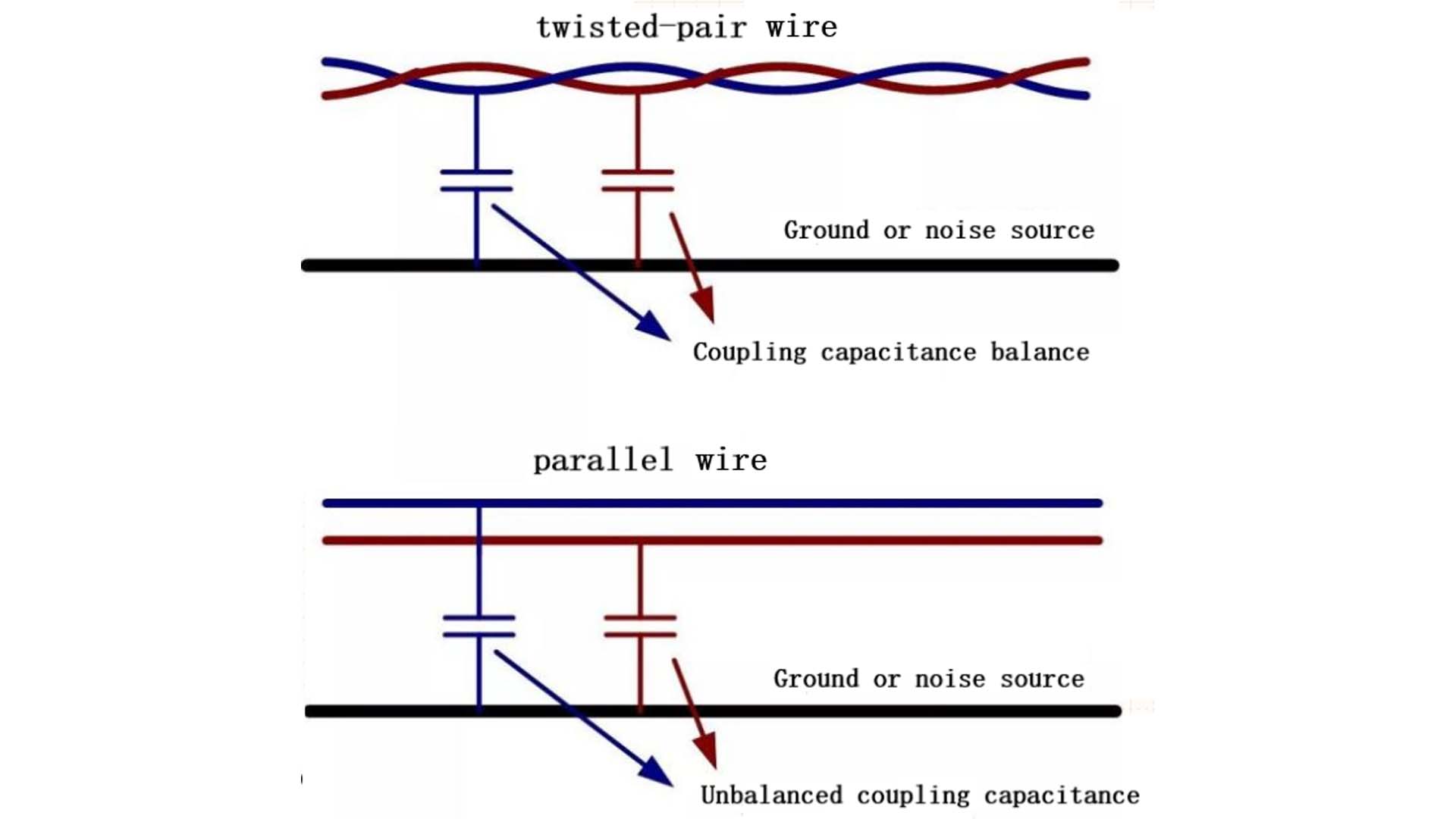
  • 1. RS422 communication principle: (1) RS422 working mode: RS422 supports full-duplex communication mode, that is, data can be transmitted bidirectionally at the same time, that is, two pairs of differential lines are used for sending and receiving respectively, which improves the efficiency and flexibility of communication. (2) Signal level: RS422 uses differential signal to transmit data, that is, two signal lines (one is a positive signal line and the other is a negative signal line) are used to transmit data. It has strong anti-interference ability and can achieve long-distance and high-speed communication. Its differential signal level standard is as follows: ① Transmitter: When transmitting logic "1", the voltage difference between line A and line B is +2V to +6V; when transmitting logic "0", the voltage difference between line A and line B is -2V to -6V. ② Receiving end: It can recognize differential voltages as low as ±200mV. When the voltage of line A is higher than the voltage of line B by more than 200mV, it is recognized as logic "1"; when the voltage of line A is lower than the voltage of line B by more than 200mV, it is recognized as logic "0". (3) Transmission distance: At 115200 baud rate, the maximum transmission distance of RS485 is usually about 1200 meters. Usually the baud rate is inversely proportional to the transmission distance, but the actual distance may vary due to the following factors: ① Transmission line quality: High-quality shielded twisted pair can reduce signal attenuation and interference and extend the transmission distance; ② Electromagnetic environment interference: An environment with strong electromagnetic interference will shorten the transmission distance; ③ Terminal matching resistance: Correctly installing the terminal resistance (usually 120 ohms) can reduce signal reflection, ensure signal integrity, and improve communication quality. If a longer distance is required, consider reducing the baud rate or using a repeater. (4) Load capacity of the transmitter: One RS422 driver can drive up to 10 receivers. (5) Connection method of terminal matching resistor: RS422 can be connected without terminal matching resistor when the distance is short (generally not more than 300 meters). When communicating over long distances, a 120 ohm resistor can be connected at the end of the signal receiving end as the terminal resistor. The terminal resistor can absorb the reflected waves on the network and effectively enhance the signal strength.   (6) Protection of RS422 circuit and suppression of interference: Generally, anti-static (ESD) protection, current limiting protection and suppression of common mode noise are required. The electrical principle is shown in the figure below:   Anti-static (ESD) protection: Connect TVS diodes to the ground on the A and B differential lines respectively to prevent static crosstalk to the subsequent circuit and damage to components. Current limiting protection: Connect a small resistance resistor in series on the A and B differential lines to prevent the signal line from short-circuiting or overcurrent from damaging the interface chip. Suppression of common mode noise: Connect common mode chokes L1 and L2 in series on the A and B differential lines to suppress common mode interference on the line and improve the anti-interference ability of the system. The common mode inductor impedance selection range is 120Ω/100MHz~2200Ω/100MHz, and the typical value is 1000Ω/100MHz. The sending and receiving A and B differential lines are connected to the ground and connected to capacitors to provide a low-impedance return path for interference to suppress common-mode high-frequency noise. The capacitance value selection range is 22PF~1000pF, and the typical value is 100pF. 2. Precautions for on-site use: (1) RS422 signal lines cannot be routed together with strong power lines, and the principle of separation of strong and weak electricity must be followed. (2) The correct connection method of signal lines and ground lines, the A and B lines of the sending end are connected to the A and B lines of the receiving end, and the ground line must also be connected. The signal ground can be an additional unshielded twisted pair or the shielding layer of a shielded twisted pair. The RS422 bus must be reliably grounded at a single point, that is, there can only be one point grounded on the entire RS422 bus, not multiple points, because the reason for grounding is to keep the voltage on the ground wire (usually the shielded wire is used as the ground wire) consistent to prevent common mode interference. If multiple points are grounded, it will be counterproductive. (3) Signal interference causes unstable communication and solutions: If there is sometimes no communication connection on site, this may be that the signal is interfered with, thus affecting the continuity of the signal. This requires the use of shielded twisted pair cables for long-distance transmission, and a 120-ohm impedance matching resistor is connected in parallel at the receiving terminal. (4) Selection of shielded cable: Choose to use ordinary Category 5e shielded twisted pair cables, i.e. network cables.   3. Common problems and solutions of RS422 communication:   Problem Possible cause Solution Communication failure Wrong line connection Ensure A+ and B- are correctly connected   Data loss Transmission distance is too long or rate is too high Reduce baud rate or use relay amplifier Severe interference Electromagnetic interference Use shielded twisted pair and ensure good grounding   Signal reflection No terminal matching Add 120Ω terminal resistor at the end of the bus Multi-device communication abnormality Exceeding the maximum number of receiving devices Reduce the number of receiving terminals or use RS-485 instead

    Read More
Prex
1 2 3 4
Next

leave a message

leave a message
If you are interested in our products and want to know more details,please leave a message here,we will reply you as soon as we can.

Home

Products

whatsApp

Contact

Shopping Cart
item.name
[[ item.product_name ]]
* [[ item.qty ]]
Your Cart Is Empty!